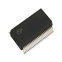
CY28159PVC Cypress Semiconductor Corp, CY28159PVC Datasheet - Page 2

CY28159PVC
Manufacturer Part Number
CY28159PVC
Description
Manufacturer
Cypress Semiconductor Corp
Datasheet
1.CY28159PVC.pdf
(13 pages)
Specifications of CY28159PVC
Function
Clock Generator
Operating Temperature (max)
70C
Operating Temperature (min)
0C
Package Type
SSOP
Pin Count
48
Mounting
Surface Mount
Lead Free Status / Rohs Status
Not Compliant
Available stocks
Company
Part Number
Manufacturer
Quantity
Price
Company:
Part Number:
CY28159PVC
Manufacturer:
CY
Quantity:
4 062
Part Number:
CY28159PVC
Manufacturer:
CYPRESS/赛普拉斯
Quantity:
20 000
Pin Description
Note:
Document #: 38-07118 Rev. *A
1.
42, 39, 36, 33
41, 38, 35, 32
24, 31, 37, 43
28, 34, 40, 47
8, 11, 14, 17,
7,10, 13, 16,
2, 6, 12, 18,
5, 9, 15, 21,
Definition of I/O column mnemonic on pin description table above 1= Input pin, O = output pin, P = power supply pin, PU = indicates that a bidirectional pin
contains pull-up resistor. This will insure that this pin of the device will be seen by the internal logic as a logic 1 level. Likewise pins with a PD designation are
guaranteed to be seen as a logic 0 level if no external level setting circuitry is present at power up.
30, 29
25, 46
27, 45
3, 4
Pin
20
26
44
48
23
22
19
1
48M(0,1), S(0,1)
SEL100/133
CPU(0:7)#
CPU(0:7)
Mult(0,1)
Name
SSCG
XOUT
VDDA
VSSA
3V33
REF
VDD
VSS
IRef
PD#
XIN
I/O
PU
PU
PU
IO
O
O
O
O
P
P
P
P
P
I
I
I
I
I
[1]
When asserted LOW, this pin invokes Spread Spectrum functionality. Spread
spectrum is applicable to CPU(0:7), CPU(0:7)#. This pin has a 250-k inter-
nal pull-up.
Differential host clock outputs. These outputs are used in pairs, (CPU0-0#,
CPU1-1#, CPU2-2#, CPU3-3#, CPU4-4#, CPU5-5#, CPU6-6#, and CPU7-7#)
for differential clocking of the host bus. CPU(0:7) are 180 degrees out of phase
with their complements, CPU(0:7)#. See Table 1 on page 1
This pin establishes the reference current for the internal current steering buff-
ers of the CPU clocks. A resistor is connected from this pin to ground to set
the value of this current.
Fixed 33.3-MHz clock output.
When asserted LOW, this pin invokes a power-down mode by shutting off all
the clocks, disabling all internal circuitry, and shutting down the crystal oscil-
lator. The 48M(0:1) and REF clocks are driven LOW during this condition and
the CPU clocks are driven HIGH and programmed with an 2X IREF current. It
has a 250-k internal pull-up.
S0 and S1 inputs are sensed on power-up and then internally latched. After-
wards the pins are 3V 48-MHz clocks.
Input select pin. See Table 1 on page 1.
It has a 250-k internal Pull-up
Crystal Buffer output pin. Connects to a crystal only. When an external signal
other than a crystal is used or when in Test mode, this pin is kept unconnected.
Crystal Buffer input pin. Connects to a crystal, or an external single ended
input clock signal.
A buffered output clock of the signal applied at Xin. Typically, 14.31818 MHz.
These input select pins configure the Ioh current (and thus the Voh swing
amplitude) of the CPU clock output pairs. Each pin has a 250-k internal
Pull-up. See Table 5 for current and resistor values.
3.3V power supply pins.
3.3V power supply pins for common supply to the core.
Ground pins for common supply to the core.
Ground pins.
Description
CY28159
Page 2 of 13
[+] Feedback


