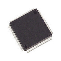
M30624FGPGP Renesas Electronics America, M30624FGPGP Datasheet - Page 68

M30624FGPGP
Manufacturer Part Number
M30624FGPGP
Description
Manufacturer
Renesas Electronics America
Datasheet
1.M30624FGPGP.pdf
(103 pages)
Specifications of M30624FGPGP
Cpu Family
M16C
Device Core Size
16/32Bit
Frequency (max)
24MHz
Interface Type
I2C/IEBus/UART
Program Memory Type
Flash
Program Memory Size
256KB
Total Internal Ram Size
20KB
# I/os (max)
87
Number Of Timers - General Purpose
11
Operating Supply Voltage (typ)
5V
Operating Supply Voltage (max)
5.5V
Operating Supply Voltage (min)
3.3V
On-chip Adc
26-chx10-bit
On-chip Dac
2-chx8-bit
Instruction Set Architecture
CISC
Mounting
Surface Mount
Pin Count
100
Package Type
LQFP
Lead Free Status / Rohs Status
Compliant
Available stocks
Company
Part Number
Manufacturer
Quantity
Price
Company:
Part Number:
M30624FGPGP
Manufacturer:
RENESAS
Quantity:
14
Part Number:
M30624FGPGP
Manufacturer:
RENESAS/瑞萨
Quantity:
20 000
Company:
Part Number:
M30624FGPGP#D3C
Manufacturer:
Renesas Electronics America
Quantity:
10 000
Company:
Part Number:
M30624FGPGP#D5C
Manufacturer:
Renesas Electronics America
Quantity:
10 000
Company:
Part Number:
M30624FGPGP#U3C
Manufacturer:
AVX
Quantity:
40 000
Company:
Part Number:
M30624FGPGP#U3C
Manufacturer:
Renesas
Quantity:
1 200
Company:
Part Number:
M30624FGPGP#U3C
Manufacturer:
Renesas Electronics America
Quantity:
10 000
Company:
Part Number:
M30624FGPGP#U5
Manufacturer:
RENESAS
Quantity:
1
Company:
Part Number:
M30624FGPGP#U5C
Manufacturer:
RENESAS
Quantity:
1 467
M16C/62P Group (M16C/62P, M16C/62PT)
Rev.2.41
REJ03B0001-0241
Table 5.31
NOTES:
I
I
I
Symbol
CC
det4
det3
1. Referenced to V
2. With one timer operated using fC32.
3. This indicates the memory in which the program to be executed exists.
4. I
specified.
det
I
I
Jan 10, 2006
det4
det3
Power Supply Current
(V
Low Voltage Detection Dissipation Current
Reset Area Detection Dissipation Current
is dissipation current when the following bit is set to “1” (detection circuit enabled).
CC1
: VC27 bit in the VCR2 register
: VC26 bit in the VCR2 register
=V
Electrical Characteristics (2)
CC2
=2.7V to 3.6V)
CC1
=V
Parameter
Page 66 of 96
CC2
=2.7 to 3.3V, V
In single-chip
mode, the output
pins are open and
other pins are V
SS
= 0V at T
(4)
(4)
SS
(1)
Mask ROM
Flash
Memory
Flash Memory
Program
Flash Memory
Erase
Mask ROM
Flash Memory
Mask ROM
Flash Memory
opr
= − 20 to 85 ° C / − 40 to 85 ° C, f(BCLK)=10MHz unless otherwise
Measuring Condition
f(BCLK)=10MHz
No division
No division,
On-chip oscillation
f(BCLK)=10MHz,
No division
No division,
On-chip oscillation
f(BCLK)=10MHz,
VCC1=3.0V
f(BCLK)=10MHz,
VCC1=3.0V
f(XCIN)=32kHz
Low power dissipation
mode, ROM
f(BCLK)=32kHz
Low power dissipation
mode, RAM
f(BCLK)=32kHz
Low power dissipation
mode, Flash Memory
On-chip oscillation,
Wait mode
f(BCLK)=32kHz
Wait mode
Oscillation capability High
f(BCLK)=32kHz
Wait mode
Oscillation capability Low
Stop mode
Topr =25 ° C
(2)
(2)
(3)
(3)
,
,
(3)
5. Electrical Characteristics
Min.
Standard
Typ.
420
1.8
6.0
1.8
0.7
0.6
0.4
12
22
25
25
45
8
1
8
Max.
3.0
11
13
4
2
Unit
mA
mA
mA
mA
mA
mA
µ A
µ A
µ A
µ A
µ A
µ A
µ A
µ A
µ A


