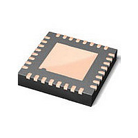
TDA18292HN/C1 NXP Semiconductors, TDA18292HN/C1 Datasheet - Page 2

TDA18292HN/C1
Manufacturer Part Number
TDA18292HN/C1
Description
Manufacturer
NXP Semiconductors
Datasheet
1.TDA18292HNC1.pdf
(2 pages)
Specifications of TDA18292HN/C1
Lead Free Status / Rohs Status
Compliant
A clear advantage
The tuner includes all the functions required to perform
digital TV reception, from RF input to baseband I/Q outputs.
It includes a balanced low-noise amplifier, complex mixer,
channel filters with built-in self calibration and a complete
RF PLL with fully integrated VCO, so no balun is required.
Programming is made easy through its I2C serial interface, and
it is possible to control two different tuners with a single line
thanks to an address select pin. A dedicated turn-on/-off pin
allows power reduction for time sliced applications and gain
is programmable in 0.5 dB steps using two up / down pins.
Making product integration easier, the PLL can operate
across a range of clock frequencies, and either a simple
crystal oscillation or a TCXO can be used for clock frequency
generation.
Evaluation kit
Our TDA18292 evaluation kit makes it simple for hardware
engineers to modify programmable settings and customize
operation. It includes tuner daughterboard, channel
decoder board for system testing, quick start guide, product
specification, application note and PC-based control software.
The tuner daughterboard can be easily connected to other
zero-IF channel decoders.
Multi-standard and multi-band capability
NXP’s TDA18292 is compliant with the following standards:
Terrestrial Digital Video Broadcast (DVB-T)
Handheld DVB (DVB-H)
Satellite services to Handheld (DVB-SH)
Terrestrial Digital Multi-media Broadcasting (T-DMB)
Integrated Services Digital Broadcasting –
It operates in the following bands and supports
1.5 / 5 / 6 / 7 / 8 MHz channel bandwidths:
VHF III (174-240MHz)
UHF (470-862MHz)
L1 (1452-1492MHz)
L2 (1670-1675MHz)
S (2170-2200MHz)
www.nxp.com
Terrestrial (ISDB-T)
© 2008 NXP B.V.
All rights reserved. Reproduction in whole or in part is prohibited without the prior written consent of the copyright owner.
The information presented in this document does not form part of any quotation or contract, is believed to be accurate and
reliable and may be changed without notice. No liability will be accepted by the publisher for any consequence of its use.
Publication thereof does not convey nor imply any license under patent- or other industrial or intellectual property rights.
L/SBANDIN
TDA18292 block diagram
System level block diagram
L-band
LNALOUT
UHF
VHF
LAGCIN
UHFIN
VHFIN
1452 MHz to
1452 MHz to
470 MHz to
174 MHz to
1492 MHz
1492 MHz
750 MHz
240 MHz
XTOUT
1
2
3
5
6
23 21
LNA
AGC
AGC
AGC
LNAUHFOUT
REFINN
REFINP
22
32
REFDIV
UHFAGCIN
16 MHz
31
TDA18292
174 MHz to
SD MODULATOR
750 MHz
MAIN DIVIDER
PFD
2nd ORDER
PLL loop filter
RF AGC
AGC
AGC
CP
CP
AGC-A
25
VTUNE
27
Date of release: January 2008
Document order number: 9397 750 16256
Printed in the Netherlands
AGCUP/AGCDN
LC VCO
I/Q base band
16 MHz
I
RXON
2
TEST1
C-bus
I/Q mixer
DIVIDER
CONTROL
I
mixer
mixer
2
28
LO
C-BUS
AGC-B
DECODER
I
AGC
2
C-BUS
FIFTH ORDER
FIFTH ORDER
AGC-A AGC-B
DECODER
CHANNEL
CONTROL
LPF
LPF
AGC
INTERFACES
TDA18292
DECODER
STANDBY
I
2
C-BUS
BB AGC
AGC
AGC
001aah152
10
11
12
13
14
17
16
15
19
9
TS/SPI/USB
I
001aah153
2
OUTIP
OUTIN
OUTQP
OUTQN
AGCUP
AGCDN
RXON
SCL
SDA
AS
C-bus


