JLC1562BN ON Semiconductor, JLC1562BN Datasheet - Page 3
JLC1562BN
Manufacturer Part Number
JLC1562BN
Description
I/O Expanders, Repeaters & Hubs I2C Bus I/O Expander
Manufacturer
ON Semiconductor
Datasheet
1.JLC1562BN.pdf
(9 pages)
Specifications of JLC1562BN
Logic Family
JLC1562
Operating Supply Voltage
4.2 V to 6 V
Package / Case
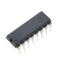
PDIP-16
Logic Type
I2C Logic
Mounting Style
Through Hole
Lead Free Status / Rohs Status
No RoHS Version Available
Available stocks
Company
Part Number
Manufacturer
Quantity
Price
Company:

Part Number:
JLC1562BN
Manufacturer:
SEK
Quantity:
2 790
Part Number:
JLC1562BN
Manufacturer:
ON/安森美
Quantity:
20 000
Company:
Part Number:
JLC1562BNG
Manufacturer:
SEMTECH
Quantity:
7 123


Î Î Î Î Î Î Î Î Î Î Î Î Î Î Î Î Î Î Î Î Î Î Î Î Î Î Î Î Î Î Î Î Î
Î Î Î Î Î Î Î Î Î Î Î Î Î Î Î Î Î Î Î Î Î Î Î Î Î Î Î Î Î Î Î Î Î
Î Î Î Î Î
Î Î Î Î Î
Î Î Î Î Î
Î Î Î Î Î
Î Î Î Î Î
Î Î Î Î Î
Î Î Î Î Î
Î Î Î Î Î
Î Î Î Î Î
Î Î Î Î Î
Î Î Î Î Î
Î Î Î Î Î
Î Î Î Î Î
Î Î Î Î Î
Î Î Î Î Î
Î Î Î Î Î
Î Î Î Î Î
Î Î Î Î Î
Î Î Î Î Î
Î Î Î Î Î
Î Î Î Î Î
Î Î Î Î Î
Î Î Î Î Î
Î Î Î Î Î
Maximum ratings are those values beyond which device damage can occur. Maximum ratings applied to the device are individual stress limit
values (not normal operating conditions) and are not valid simultaneously. If these limits are exceeded, device functional operation is not implied,
damage may occur and reliability may be affected.
RECOMMENDED OPERATING CONDITIONS
DC CHARACTERISTICS
COMPARATOR AC CHARACTERISTICS
MAXIMUM RATINGS (Referenced to GND)
Symbol
Symbol
V
Symbol
Symbol
in
V
V
C
T
V
V
I
V
V
C
V
C
I
t
V
I
T
, V
T
DD
I
CC
PD
ICR
stg
oz
out
OL
out
dd
I
dd
in
IH
i/o
in
A
IL
L
in
out
Î Î Î Î Î Î Î Î Î Î Î Î Î Î Î Î Î Î Î
Î Î Î Î Î Î Î Î Î Î Î Î Î Î Î Î Î Î Î
Î Î Î Î Î Î Î Î Î Î Î Î Î Î Î Î Î Î Î
Î Î Î Î Î Î Î Î Î Î Î Î Î Î Î Î Î Î Î
Î Î Î Î Î Î Î Î Î Î Î Î Î Î Î Î Î Î Î
Î Î Î Î Î Î Î Î Î Î Î Î Î Î Î Î Î Î Î
Î Î Î Î Î Î Î Î Î Î Î Î Î Î Î Î Î Î Î
Î Î Î Î Î Î Î Î Î Î Î Î Î Î Î Î Î Î Î
Î Î Î Î Î Î Î Î Î Î Î Î Î Î Î Î Î Î Î
Î Î Î Î Î Î Î Î Î Î Î Î Î Î Î Î Î Î Î
Î Î Î Î Î Î Î Î Î Î Î Î Î Î Î Î Î Î Î
Î Î Î Î Î Î Î Î Î Î Î Î Î Î Î Î Î Î Î
Î Î Î Î Î Î Î Î Î Î Î Î Î Î Î Î Î Î Î
Î Î Î Î Î Î Î Î Î Î Î Î Î Î Î Î Î Î Î
Î Î Î Î Î Î Î Î Î Î Î Î Î Î Î Î Î Î Î
Î Î Î Î Î Î Î Î Î Î Î Î Î Î Î Î Î Î Î
Î Î Î Î Î Î Î Î Î Î Î Î Î Î Î Î Î Î Î
Î Î Î Î Î Î Î Î Î Î Î Î Î Î Î Î Î Î Î
Î Î Î Î Î Î Î Î Î Î Î Î Î Î Î Î Î Î Î
Î Î Î Î Î Î Î Î Î Î Î Î Î Î Î Î Î Î Î
Î Î Î Î Î Î Î Î Î Î Î Î Î Î Î Î Î Î Î
Î Î Î Î Î Î Î Î Î Î Î Î Î Î Î Î Î Î Î
Î Î Î Î Î Î Î Î Î Î Î Î Î Î Î Î Î Î Î
Î Î Î Î Î Î Î Î Î Î Î Î Î Î Î Î Î Î Î
DC Supply Voltage
DC Input Voltage
Operating Temperature
Maximum Input Voltage, “H”
Maximum Input Voltage, “L”
Maximum Output Voltage, “L” (I
Maximum Input Leakage Current (V
Maximum Output Hi−Z Leakage Current (Output = High Impedance; V
Maximum Input Capacitance (Input Pin)
Maximum Output Capacitance (Output Pin)
Maximum I/O Capacitance (I/O Pin)
Comparator Common Mode Input Voltage Range
Maximum Quiescent Supply Current (per Package)
Maximum Propagation Delay
DC Supply Voltage
DC Input Voltage
DC Output Voltage
DC Input/Output Current (per Pin)
DC Supply Current (V
Storage Temperature Range
Lead Temperature, 1 mm from Case for 10 Seconds
(Referenced to V
Parameter
DD
and GND Pins)
out
ss
)
Parameter
Parameter
Parameter
= 4mA)
in
= V
dd
http://onsemi.com
or V
V
V
JLC1562B
ss
ref
ref
, SCL pin only)
= 1.5 V, 100mV overdrive
= 1.5 V, 10mV overdrive
Test Conditions
3
out
= V
dd
Î Î Î Î Î Î Î Î
Î Î Î Î Î Î Î Î
Î Î Î Î Î Î Î Î
Î Î Î Î Î Î Î Î
Î Î Î Î Î Î Î Î
Î Î Î Î Î Î Î Î
Î Î Î Î Î Î Î Î
Î Î Î Î Î Î Î Î
Î Î Î Î Î Î Î Î
Î Î Î Î Î Î Î Î
Î Î Î Î Î Î Î Î
Î Î Î Î Î Î Î Î
Î Î Î Î Î Î Î Î
Î Î Î Î Î Î Î Î
Î Î Î Î Î Î Î Î
Î Î Î Î Î Î Î Î
Î Î Î Î Î
Î Î Î Î Î
Î Î Î Î Î
Î Î Î Î Î
Î Î Î Î Î
Î Î Î Î Î
Î Î Î Î Î
Î Î Î Î Î
)
Min
0.7 V
−
−
Min
–40
Min
Guaranteed Limit
Guaranteed Limit
4.2
0.0
–0.5 to V
–0.5 to V
−
−
−
−
−
−
−
0
−
–0.5 to +7.0
–65 to +150
dd
Value
Typ
300
1.0
0.2
Î Î Î Î
Î Î Î Î
Î Î Î Î
Î Î Î Î
Î Î Î Î
Î Î Î Î
Î Î Î Î
Î Î Î Î
25
75
dd
dd
V
+0.5
+0.5
0.3 V
dd
± 1.0
± 5.0
Max
Max
V
+85
6.0
0.3
5.0
10
15
15
−
dd
−1.5
Max
dd
−
−
Î Î Î Î
Î Î Î Î
Î Î Î Î
Î Î Î Î
Î Î Î Î
Î Î Î Î
Î Î Î Î
Î Î Î Î
Î Î Î Î
Î Î Î Î
Î Î Î Î
Î Î Î Î
Î Î Î Î
Î Î Î Î
Î Î Î Î
Î Î Î Î
Î Î Î Î
Î Î Î Î
Î Î Î Î
Î Î Î Î
Î Î Î Î
Î Î Î Î
Î Î Î Î
Î Î Î Î
Unit
Unit
Unit
Unit
mA
mA
mA
mA
mA
pF
pF
pF
mS
mS
°C
°C
°C
V
V
V
V
V
V
V
V
V
Related parts for JLC1562BN
Image
Part Number
Description
Manufacturer
Datasheet
Request
R

Part Number:
Description:
ON Semiconductor [VOLTAGE REGULATOR]
Manufacturer:
ON Semiconductor
Datasheet:
Part Number:
Description:
357-036-542-201 CARDEDGE 36POS DL .156 BLK LOPRO
Manufacturer:
ON Semiconductor
Datasheet:
Part Number:
Description:
357-036-542-201 CARDEDGE 36POS DL .156 BLK LOPRO
Manufacturer:
ON Semiconductor
Datasheet:
Part Number:
Description:
357-036-542-201 CARDEDGE 36POS DL .156 BLK LOPRO
Manufacturer:
ON Semiconductor
Datasheet:
Part Number:
Description:
357-036-542-201 CARDEDGE 36POS DL .156 BLK LOPRO
Manufacturer:
ON Semiconductor
Datasheet:
Part Number:
Description:
357-036-542-201 CARDEDGE 36POS DL .156 BLK LOPRO
Manufacturer:
ON Semiconductor
Datasheet:
Part Number:
Description:
357-036-542-201 CARDEDGE 36POS DL .156 BLK LOPRO
Manufacturer:
ON Semiconductor
Datasheet:
Part Number:
Description:
357-036-542-201 CARDEDGE 36POS DL .156 BLK LOPRO
Manufacturer:
ON Semiconductor
Datasheet:
Part Number:
Description:
357-036-542-201 CARDEDGE 36POS DL .156 BLK LOPRO
Manufacturer:
ON Semiconductor
Datasheet:
Part Number:
Description:
357-036-542-201 CARDEDGE 36POS DL .156 BLK LOPRO
Manufacturer:
ON Semiconductor
Datasheet:
Part Number:
Description:
357-036-542-201 CARDEDGE 36POS DL .156 BLK LOPRO
Manufacturer:
ON Semiconductor
Datasheet:
Part Number:
Description:
Manufacturer:
ON Semiconductor
Datasheet:
Part Number:
Description:
Manufacturer:
ON Semiconductor
Datasheet:
Part Number:
Description:
Manufacturer:
ON Semiconductor
Datasheet: