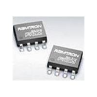
FM24CL64-G Ramtron, FM24CL64-G Datasheet - Page 6

FM24CL64-G
Manufacturer Part Number
FM24CL64-G
Description
F-RAM 64K (8Kx8) 2.7V
Manufacturer
Ramtron
Datasheet
1.FM24CL64-G.pdf
(13 pages)
Specifications of FM24CL64-G
Memory Size
64 KB
Organization
8 K x 8
Interface
2-Wire
Operating Supply Voltage
2.7 V to 3.6 V
Operating Temperature Range
- 40 C to + 85 C
Package / Case
SOIC-8
Mounting Style
SMD/SMT
Lead Free Status / Rohs Status
Details
Available stocks
Company
Part Number
Manufacturer
Quantity
Price
Part Number:
FM24CL64-G
Manufacturer:
RAMTRON
Quantity:
20 000
Company:
Part Number:
FM24CL64-GTR
Manufacturer:
ramtron
Quantity:
10 000
Part Number:
FM24CL64-GTR
Manufacturer:
RAMTROM
Quantity:
20 000
Read Operation
There are two basic types of read operations. They
are current address read and selective address read. In
a current address read, the FM24CL64 uses the
internal address latch to supply the address. In a
selective read, the user performs a procedure to set
the address to a specific value.
Current Address & Sequential Read
As mentioned above the FM24CL64 uses an internal
latch to supply the address for a read operation. A
current address read uses the existing value in the
address latch as a starting place for the read
operation. The system reads from the address
immediately following that of the last operation.
To perform a current address read, the bus master
supplies a device address with the LSB set to 1. This
indicates that a read operation is requested. After
receiving
FM24CL64 will begin shifting out data from the
current address on the next clock. The current address
is the value held in the internal address latch.
Beginning with the current address, the bus master
can read any number of bytes. Thus, a sequential read
is simply a current address read with multiple byte
transfers. After each byte the internal address counter
will be incremented.
Rev. 3.4
Feb. 2011
By FM24CL64
By FM24CL64
Each time the bus master acknowledges a byte,
this indicates that the FM24CL64 should read
out the next sequential byte.
By Master
By Master
Start
S
the
Start
S
Slave Address
complete
Slave Address
0
device
A
Address & Data
Address MSB
0
address,
A
Figure 6. Multiple Byte Write
Figure 5. Single Byte Write
Address & Data
Acknowledge
Address MSB
the
A
Address LSB
Acknowledge
A
There are four ways to properly terminate a read
operation. Failing to properly terminate the read will
most likely create a bus contention as the FM24CL64
attempts to read out additional data onto the bus. The
four valid methods are:
1.
2.
3.
4.
If the internal address reaches 1FFFh, it will wrap
around to 0000h on the next read cycle. Figures 7 and
8 below show the proper operation for current
address reads.
Selective (Random) Read
There is a simple technique that allows a user to
select a random address location as the starting point
for a read operation. This involves using the first
three bytes of a write operation to set the internal
address followed by subsequent read operations.
To perform a selective read, the bus master sends out
the device address with the LSB set to 0. This
specifies a write operation. According to the write
protocol, the bus master then sends the address bytes
that are loaded into the internal address latch. After
the FM24CL64 acknowledges the address, the bus
master issues a start condition. This simultaneously
The bus master issues a no-acknowledge in the
9
This is illustrated in the diagrams below. This is
preferred.
The bus master issues a no-acknowledge in the
9
The bus master issues a stop in the 9
cycle.
The bus master issues a start in the 9
cycle.
th
th
Address LSB
A
clock cycle and a start in the 10
clock cycle and a stop in the 10
Data Byte
A
A
Data Byte
Data Byte
th
th
.
FM24CL64
clock cycle.
Page 6 of 13
A
th
th
A
Stop
P
Stop
clock
clock
P


