H57V2562GTR-75C HYNIX SEMICONDUCTOR, H57V2562GTR-75C Datasheet
H57V2562GTR-75C
Specifications of H57V2562GTR-75C
Available stocks


Related parts for H57V2562GTR-75C

H57V2562GTR-75C Summary of contents
Page 1
Synchronous DRAM based 4Bank x16 I/O 256M (16Mx16bit) Hynix SDRAM - Organized as 4banks of 4,194,304 x 16 This document is a general product description and is subject to change without notice. Hynix does not assume ...
Page 2
... Synchronous DRAM Revision History Revision No. 0.1 1.0 Release (Update PKG dimension raw data) Rev 1.0 / Dec. 2010 Synchronous DRAM Memory 256Mbit H57V2562GTR Document Title History Preliminary H57V2562GTR Series Draft Date Remark Jun. 2009 Dec. 2010 2 ...
Page 3
... DESCRIPTION The Hynix H57V2562GTR Synchronous DRAM is 268,435,456bit CMOS Synchronous DRAM, ideally suited for the con- sumer memory applications which requires large memory density and high bandwidth organized as 4banks of 4,194,304 x 16 I/O. Synchronous DRAM is a type of DRAM which operates in synchronization with input clock. The Hynix Synchronous DRAM latch each control signal at the rising edge of a basic input clock (CLK) and input/output data in synchronization with the input clock (CLK) ...
Page 4
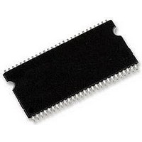
... Package Type : 54_Pin TSOPII ● This product is in compliance with the directive pertaining of RoHS. ● ORDERING INFORMATION Clock Part Number Frequency H57V2562GTR-60C 166MHz H57V2562GTR-75C 133MHz H57V2562GTR-50C 200MHz H57V2562GTR-60L 166MHz H57V2562GTR-75L 133MHz H57V2562GTR-50L 200MHz Note: 1. H57V2562GTR-XXC Series: Normal power & Commercial temp. ...
Page 5
... LDQM 15 /WE 16 /CAS 17 /RAS 18 /CS 19 BA0 20 BA1 21 A10/ VDD 27 Rev 1.0 / Dec. 2010 Synchronous DRAM Memory 256Mbit 54 Pin TSOPII 400mil x 875mil 0.8mm pin pitch H57V2562GTR Series VSS 54 DQ15 53 VSSQ 52 DQ14 51 DQ13 50 VDDQ 49 DQ12 48 DQ11 47 VSSQ 46 DQ10 45 DQ9 44 VDDQ 43 DQ8 42 VSS UDQM ...
Page 6
... DQ0 ~ DQ15 I/O Multiplexed data input / output pin SUPPLY Power supply for internal circuits and input buffers SUPPLY Power supply for output buffers DDQ SSQ connection : These pads should be left unconnected Rev 1.0 / Dec. 2010 Synchronous DRAM Memory 256Mbit H57V2562GTR Series DESCRIPTION 6 ...
Page 7
... Synchronous DRAM Memory 256Mbit Internal Row Counter 4M x16 Bank3 Row Pre Decoder Column Pre Decoder Column Add Counter Burst Counter CAS Latency Mode Register H57V2562GTR Series 4M x16 Bank2 4M x16 Bank1 4M x16 Bank0 Memory Cell Array Y decoerders Pipe Line Control Data Out Control DQ0 DQ15 7 ...
Page 8
... Rev 1.0 / Dec. 2010 Synchronous DRAM Memory 256Mbit Symbol STG OUT DDQ Symbol Min 3.0 DD DDQ Symbol trip outref CL H57V2562GTR Series Rating -55 ~ 125 -1.0 ~ 4.6 -1 Max Unit 3 0.3 V DDQ 0.8 V =3.30. =0V Value Unit 2 Unit Note Note 1 ...
Page 9
... Rev 1.0 / Dec. 2010 Synchronous DRAM Memory 256Mbit VTT = 1. Ohom Output 50pF Pin ( Symbol Min 2 H57V2562GTR Series VTT = 1. Ohom Ohom 50pF AC Output Load Circuit Symbol Min Max CI1 2.0 4.0 CI2 2.0 4.0 CI3 2.0 4.0 CI/O 3.5 6.5 Max Unit Note 1 uA ...
Page 10
... DD6 Current Note and I depend on output loading and cycle rates. Specified values are measured with the output open. DD1 DD4 2. Min. of tRC (Refresh RAS cycle time) is shown at AC CHARACTERISTICS II 3. H57V2562GTR-XXC Series: Normal, Rev 1.0 / Dec. 2010 (TA Test Condition t (min), I ...
Page 11
... CKS t 0.8 - 0.8 CKH t 1 0 1.0 - 1.0 OLZ t - 4.5 2.7 OHZ3 OHZ2 & t > 1ns, then [(t +t )/2-1]ns should be added to the parameter H57V2562GTR Series 166 133 Unit Max Min Max 1000 7.5 1000 ns 1000 10 1000 5 0.8 ...
Page 12
... Min RRC RCD t 38.7 100K RAS RRD CCD WTL DPL t DAL DQZ DQM MRD PROZ3 PROZ2 DPE SRE REF after self refresh exit. RC H57V2562GTR Series 166 133 Unit Max Min Max 100K 42 100K CLK CLK CLK DPL CLK CLK CLK CLK - - 2 ...
Page 13
... Reserved Reserved Reserved Reserved Reserved Rev 1.0 / Dec. 2010 Code 0 0 Burst Length Synchronous DRAM Memory 256Mbit H57V2562GTR Series CAS Latency BT Burst Length Burst Type A3 Burst Type 0 Sequential 1 Interleave Burst Length Reserved 0 1 Reserved 1 0 Reserved 1 1 Full page A1 A0 ...
Page 14
... Note : 1. Exiting Self Refresh occurs by asynchronously bringing CKE from low to high. 2. see to Next page (DQM TRUTH TABLE) Rev 1.0 / Dec. 2010 CKEn CS RAS CAS Synchronous DRAM Memory 256Mbit H57V2562GTR Series A10 WE DQM ADDR / Code Row Address Col umn Col umn Col umn Col umn Pin High (Other Pins OP code ...
Page 15
... Lower byte Mask/Output disable, Upper byte write/Output enable Note 1. H: High Level, L: Low Level, X: Don 2. Write DQM Latency is 0 CLK and Read DQM Latency is 2 CLK Rev 1.0 / Dec. 2010 Synchronous DRAM Memory 256Mbit CKEn-1 CKEn Care H57V2562GTR Series LDQM UDQM ...
Page 16
... Precharge BA Row Add. Bank Activate Col Add. BA Write/WriteAP A10 Col Add. BA Read/ReadAP A10 Operation H57V2562GTR Series Action Notes Set the Mode Register Start Auto or Self Refresh 5 No Operation Activate the specified bank and row ILLEGAL 4 ILLEGAL 4 No Operation 3 No Operation or Power ...
Page 17
... X Precharge BA Row Add. Bank Activate BA Col Add. A10 Write/WriteAP BA Col Add. A10 Read/ReadAP Operation X X Device Deselect H57V2562GTR Series Action Notes Continue the Burst ILLEGAL 13 13 Termination Burst: Start 10 the Precharge ILLEGAL 4 Termination Burst: Start 8 Write(optional AP) Termination Burst: Start 8,9 Read(optional AP) ...
Page 18
... X X Auto or Self Refresh ILLEGAL BA X Precharge BA Row Add. Bank Activate BA Col Add. A10 Write/WriteAP BA Col Add. A10 Read/ReadAP Operation H57V2562GTR Series Action Notes ILLEGAL Operation: Bank(s) idle after t RP ILLEGAL 4,12 ILLEGAL 4,12 ILLEGAL 4,12 No Operation: Bank(s) idle after t RP ...
Page 19
... Auto or Self Refresh ILLEGAL BA X Precharge BA Row Add. Bank Activate BA Col Add. A10 Write/WriteAP BA Col Add. A10 Read/ReadAP Operation X X Device Deselect H57V2562GTR Series Action Notes No Operation: Row Active after t DPL ILLEGAL 13 13 ILLEGAL 4,13 ILLEGAL 4,12 ILLEGAL 4,12 ILLEGAL 4,9,12 No Operation: Precharge after t ...
Page 20
... Must mask preceding data which don 11. Illegal not satisfied RRD 12. Illegal for single bank, but legal for other banks in multi-bank devices. 13. Illegal for all banks. Rev 1.0 / Dec. 2010 ' t care, BA: Bank Address, AP: Auto Precharge satisfy t . DPL Synchronous DRAM Memory 256Mbit H57V2562GTR Series 20 ...
Page 21
... CODE CODE H57V2562GTR Series Action ADDR X INVALID Exit Self Refresh with X Device Deselect Exit Self Refresh with X No Operation X ILLEGAL X ILLEGAL X ILLEGAL X Maintain Self Refresh X INVALID X Power Down mode exit, all banks idle ILLEGAL X X Maintain Power Down Mode Refer to the idle State section ...
Page 22
... CKE goes high and is maintained for a minimum 200usec. Rev 1.0 / Dec. 2010 Synchronous DRAM Memory 256Mbit (Sheet Command BA0, CS RAS CAS WE BA1 H57V2562GTR Series Action ADDR Refer to operations of X the Current State Truth Table Begin Clock Suspend X next cycle Exit Clock Suspend X next cycle X Maintain Clock Suspend Notes 22 ...
Page 23
... Synchronous DRAM Memory 256Mbit H57V2562GTR Series A1 inches Min Typ 0.0390 0.0020 0.0039 0.0374 0.0394 0.012 - 0.0047 - 0.0039 0.8720 0.8748 0.4620 0.4630 0.3950 0 ...