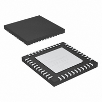
MAX9671CTH+T Maxim Integrated Products, MAX9671CTH+T Datasheet - Page 3

MAX9671CTH+T
Manufacturer Part Number
MAX9671CTH+T
Description
IC AUDIO/VIDEO SWIT DUAL 44TQFN
Manufacturer
Maxim Integrated Products
Datasheet
1.MAX9670CTL.pdf
(44 pages)
Specifications of MAX9671CTH+T
Function
Audio/Video Switch
Circuit
2 x SCART
Voltage Supply Source
Single Supply
Voltage - Supply, Single/dual (±)
3.3 V ~ 12 V
Operating Temperature
0°C ~ 70°C
Mounting Type
Surface Mount
Package / Case
44-TQFN Exposed Pad
For Use With
MAX9671EVKIT+ - EVALUATION KIT FOR MAX9671
Lead Free Status / RoHS Status
Lead free / RoHS Compliant
ELECTRICAL CHARACTERISTICS (continued)
(V
T
AC-COUPLED INPUT
Sync-Tip Clamp Level
Sync Crush
Input Clamping Current
Maximum Input Source
Resistance
Input Voltage
Input Resistance
DC CHARACTERISTICS
DC Voltage Gain
DC Gain Mismatch Among R, G,
and B Outputs
Output Level
Output Voltage Swing
Output Short-Circuit Current
Output Resistance
Output Leakage Current
Power-Supply Rejection Ratio
A
12
= +25°C.) (Note 2)
= 12V, V
PARAMETER
Volume Control for Dual SCART Connectors
VID
Low-Power Audio/Video Switch with Audio
= V
_______________________________________________________________________________________
AUD
= 3.3V, V
GNDVID
SYMBOL
R
V
A
CLP
OUT
V
= V
EP
Sync-tip clamp
S ync- ti p cl am p ; p er centag e r ed ucti on i n
sync p ul se ( 0.3V
cl am p i ng cur r ent m easur em ent, T
Sync-tip clamp, V
Input sync-tip circuit must be stable even if
the source resistance is as high as 300Ω
Bias circuit
High-impedance input circuit
Bias circuit
High-impedance input circuit
Guaranteed by output voltage swing
Guaranteed by output voltage swing of
TV_R/C_OUT, TV_G_OUT, and TV_B_OUT;
first input signal set is VCR_R/C_IN,
VCR_G_IN, and VCR_B_IN; second signal
set is ENC_R/C_IN, ENC_G_IN, and
ENC_B_IN
Sync-tip clamp (V
Bias circuit
Sync-tip clamp, measured at output,
V
R
Measured at output, V
V
V
Bias circuit, measured at output, V
V
R
Measured at output, V
V
R
Output disabled (load detection not active)
3V ≤ V
= 0V, no load, T
VID
CLP
VID
IN
IN
L
L
L
= 150Ω to V
= 150Ω to V
= 150Ω to V
= (V
= (V
/2, R
= 3V, V
to (V
VID
BIAS
BIAS
L
≤ 3.6V
CLP
= 75Ω to GNDVID
IN
- 0.575V) to (V
- 0.575V) to (V
+ 1.15V), R
= V
CONDITIONS
VID
VID
VID
P - P
IN
IN
A
/2, R
/2, R
/2, R
CLP
) ; g uar anteed b y i np ut
= 0°C to +70°C, unless otherwise noted. Typical values are at
= 0.3V, T
= V
VID
VID
to (V
L
L
L
CLP
= 75Ω to GNDVID
= 75Ω to GNDVID
= 75Ω to GNDVID
= 3.135V, V
L
= 3.135V,
CLP
)
= 150Ω to
BIAS
BIAS
A
= +25°C
+1.15V),
+ 0.575V),
+ 0.575V),
A
VID
= + 25° C
IN
= 3V,
=
2.243
2.243
0.3 x
0.57
V
1.95
MIN
-13
0.1
1.3
35
-2
VID
TYP
0.30
300
222
100
0.6
1.5
2.3
2.3
2.3
2.3
0.5
10
-4
1
2
0.36 x
2.358
2.358
MAX
0.63
V
2.05
0.51
1.78
170
+6
+2
VID
2
2
UNITS
V
mV
V/V
mA
kΩ
µA
µA
dB
%
%
Ω
P-P
Ω
V
V
3


