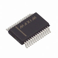
MAX4550CAI+T Maxim Integrated Products, MAX4550CAI+T Datasheet - Page 6

MAX4550CAI+T
Manufacturer Part Number
MAX4550CAI+T
Description
IC CROSSPOINT SWITCH DUAL 28SSOP
Manufacturer
Maxim Integrated Products
Datasheet
1.MAX4570EAI.pdf
(16 pages)
Specifications of MAX4550CAI+T
Function
Audio/Video Crosspoint Switch
Circuit
2 x 4:2
On-state Resistance
100 Ohm
Voltage Supply Source
Single, Dual Supply
Voltage - Supply, Single/dual (±)
2.7 V ~ 5.5 V, ±2.7 V ~ 5.5 V
Current - Supply
7µA
Operating Temperature
0°C ~ 70°C
Mounting Type
Surface Mount
Package / Case
28-SSOP
Lead Free Status / RoHS Status
Lead free / RoHS Compliant
Serially Controlled, Dual 4x2, Clickless
Audio/Video Analog Crosspoint Switches
INTERFACE I/O CHARACTERISTICS (continued)
(V+ = +2.7V to +5.5V, V- = 0 to -5.5V, T
(T
6
Note 2: The algebraic convention is used in this data sheet; the most negative value is shown in the minimum column.
Note 3: Guaranteed by design. Not subject to production testing.
Note 4: ∆R
Note 5: On-resistance flatness is defined as the difference between the maximum and minimum on-resistance values, as measured
Note 6: Leakage parameters are 100% tested at maximum rated temperature, and guaranteed by correlation at T
Note 7: Off-isolation = 20
Note 8: All timing is measured from the clock’s falling edge preceding the ACK signal for 2-wire, and from CS’s rising edge for
Note 9: Typical values are for MAX4570 only.
Note 10: Supply current can be as high as 2mA per switch during switch transitions in the clickless mode, corresponding to 40mA
Note 11: Leakage testing for single-supply operation is guaranteed by testing with dual supplies.
Note 12: Cb = capacitance of one bus line in pF. Tested with Cb = 400pF.
SCLK Pulse Width Low
SCLK Pulse Width High
Rise Time (SCLK, DIN, CS)
Fall Time (SCLK, DIN, CS)
A
= +25°C, unless otherwise noted.)
_______________________________________________________________________________________
60
58
56
54
52
50
48
46
44
42
40
-5
over the specified analog signal range.
3-wire. Turn-Off Time is defined as the output of the switch for 0.5V change, tested with a 300Ω load to ground. Turn-On
Time is measured with a 5kΩ load resistor to GND. All timing is shown with respect to 20% of V+ and 70% of V+, unless
otherwise noted.
total supply transient current requirement.
PARAMETER
-4
ON
ON-RESISTANCE vs. V
-3 -2 -1
= R
(DUAL SUPPLIES)
ON(MAX)
V
V± = ±4.75V
COM
V± = ±2.7V
V± = ±3.3V
0
(V)
·
1
- R
log (V
2
ON(MIN)
COM
3
COM_ __
SYMBOL
4
t
t
.
CH
A
CL
t
t
R
F
5
= T
/ V
MIN
NO_ _
to T
55
50
40
35
60
45
30
), V
-5
MAX
AND TEMPERATURE (DUAL SUPPLIES)
V± = ±5V
COM_ _
-4
, unless otherwise noted. Typical values are at T
ON-RESISTANCE vs. V
-3 -2 -1
= output, V
CONDITIONS
V
T
T
T
A
COM
T
A
A
A
= +25°C
= -40°C
0
= +85°C
= +70°C
(V)
Typical Operating Characteristics
1
NO_ _
2
COM
3
= input to off switch.
4
5
130
120
110
100
90
80
70
60
50
0
MIN
200
200
ON-RESISTANCE vs. V
1
A
= +25°C.) (Note 2)
(SINGLE SUPPLY)
TYP
V+ = +2.7V
2
V
COM
A
(V)
MAX
= +25°C.
3
2.0
2.0
V+ = +3.3V
COM
V+ = +5V
4
UNITS
ns
ns
µs
µs
5


