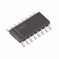
MAX9152ESE+ Maxim Integrated Products, MAX9152ESE+ Datasheet - Page 2

MAX9152ESE+
Manufacturer Part Number
MAX9152ESE+
Description
IC CROSSPOINT SWITCH 2X2 16SOIC
Manufacturer
Maxim Integrated Products
Datasheet
1.MAX9152EUE.pdf
(12 pages)
Specifications of MAX9152ESE+
Function
Crosspoint Switch
Circuit
1 x 2:2
Voltage Supply Source
Single Supply
Voltage - Supply, Single/dual (±)
3 V ~ 3.6 V
Operating Temperature
-40°C ~ 85°C
Mounting Type
Surface Mount
Package / Case
16-SOIC (0.154", 3.90mm Width)
Lead Free Status / RoHS Status
Lead free / RoHS Compliant
ABSOLUTE MAXIMUM RATINGS
V
IN_+, IN_-, OUT_+, OUT_- to GND .......................-0.3V to +4.0V
EN_, SEL_, NC/RSEL to GND.....................-0.3V to (V
Short-Circuit Duration (OUT_+, OUT_-) .....................Continuous
Continuous Power Dissipation (T
800Mbps LVDS/LVPECL-to-LVDS 2 x 2
Crosspoint Switch
Stresses beyond those listed under “Absolute Maximum Ratings” may cause permanent damage to the device. These are stress ratings only, and functional
operation of the device at these or any other conditions beyond those indicated in the operational sections of the specifications is not implied. Exposure to
absolute maximum rating conditions for extended periods may affect device reliability.
DC ELECTRICAL CHARACTERISTICS
(V
0.1V to V
V
2
CC
CC
Input High Voltage
Input Low Voltage
Input High Current
Input Low Current
NC/RSEL INPUT
Input High Voltage
Input Low Voltage
Input High Current
Input Low Current
Differential Input High Threshold
Differential Input Low Threshold
Input Current
Differential Output Impedance
(Note 2)
Differential Output Voltage
Change in Magnitude of V
Between Complementary Output
States
Offset Common-Mode Voltage
Change in Magnitude of V
Between Complementary Output
States
LVCMOS/LVTTL INPUTS (EN_, SEL_)
DIFFERENTIAL INPUTS (IN_+, IN_-)
LVDS OUTPUTS (OUT_+, OUT_-)
CC
16-Pin SO (derate 8.7mW/°C above +70°C)................696mW
16-Pin TSSOP (derate 9.4mW/°C above +70°C) .........755mW
_______________________________________________________________________________________
to GND ...........................................................-0.3V to +4.0V
= +3.3V, |V
= +3.0V to +3.6V, NC/RSEL = open for R
CC
PARAMETER
, input voltage (V
ID
| = 0.2V, input common-mode voltage V
OD
OS
IN+
, V
A
= +70°C)
IN-
) = 0 to V
SYMBOL
I
IN+,
∆V
R
∆V
V
V
V
V
V
V
V
V
I
I
DIFF
I
I
OD
IH
IH
TH
OS
IL
IL
TL
IH
IH
IL
IL
OD
OS
I
IN-
CC
L
, EN_ = high, SEL0 = low, SEL1 = high, and T
= 75Ω ±1%, NC/RSEL = high for R
V
V
V
V
V
V
V
NC/RSEL = low or open
NC/RSEL = high
R
R
R
R
R
R
R
R
CC
IN
IN
IN
IN
IN+
I N +
C C
L
L
L
L
L
L
L
L
= 75Ω, NC/RSEL = open, Figure 1
= 100Ω, NC/RSEL = high, Figure 1
= 75Ω, NC/RSEL = open, Figure 1
= 100Ω, NC/RSEL = high, Figure 1
= 75Ω, NC/RSEL = open, Figure 1
= 100Ω, NC/RSEL = high, Figure 1
= 75Ω, NC/RSEL = open, Figure 1
= 100Ω, NC/RSEL = high, Figure 1
= V
= 0 or 0.8V
= V
= 0 or 0.8V
+ 0.3V)
= V
= 3. 6 V o r 0 , V
= 0
CM
CC
CC
CC
= 1.2V, T
or 2.0V
or 2.0V
or 0, V
CONDITIONS
Storage Temperature Range .............................-65°C to +150°C
Junction Temperature ......................................................+150°C
Operating Temperature Range ...........................-40°C to +85°C
Lead Temperature (soldering, 10s) .................................+300°C
ESD Protection
IN-
A
I N -
= +25°C, unless otherwise noted.) (Note 1)
Human Body Model, IN_+, IN_-, OUT_+, OUT_-........... ±7kV
= V
= 3 . 6 V or 0 ,
CC
or 0
L
= 100Ω ±1%, differential input voltage |V
A
= -40°C to +85°C. Typical values at
1.150
GND
GND
MIN
-100
280
-10
-10
60
85
-1
-1
2.0
2.0
0
0
TYP
122
382
90
1.430
MAX
V
V
100
118
155
470
0.8
0.8
20
10
20
10
25
CC
CC
1
1
25
UNITS
mV
mV
mV
mV
mV
µA
µA
µA
µA
µA
Ω
V
V
V
V
V
ID
| =


