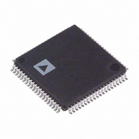
AD8109AST Analog Devices Inc, AD8109AST Datasheet - Page 19

AD8109AST
Manufacturer Part Number
AD8109AST
Description
IC VIDEO CROSSPOINT SWIT 80LQFP
Manufacturer
Analog Devices Inc
Datasheet
1.AD8109ASTZ.pdf
(32 pages)
Specifications of AD8109AST
Rohs Status
RoHS non-compliant
Function
Video Crosspoint Switch
Circuit
1 x 8:8
Voltage Supply Source
Dual Supply
Voltage - Supply, Single/dual (±)
±4.5 V ~ 5.5 V
Operating Temperature
-40°C ~ 85°C
Mounting Type
Surface Mount
Package / Case
80-LQFP
Array Configuration
8x8
Number Of Arrays
1
Screening Level
Industrial
Pin Count
80
Package Type
LQFP
Power Supply Requirement
Dual
Lead Free Status / RoHS Status
Not Compliant
Available stocks
Company
Part Number
Manufacturer
Quantity
Price
Company:
Part Number:
AD8109ASTZ
Manufacturer:
ADI
Quantity:
158
Company:
Part Number:
AD8109ASTZ
Manufacturer:
Analog Devices Inc
Quantity:
10 000
Part Number:
AD8109ASTZ
Manufacturer:
ADI/亚德诺
Quantity:
20 000
AD8108/AD8109. When taken low, the RESET signal will only
set each output to the disabled state. This is helpful during
power-up to ensure that two parallel outputs will not be active
at the same time.
After initial power-up, the internal registers in the device will
generally have random data, even though the RESET signal was
asserted. If parallel programming is used to program one
output, that output will be properly programmed, but the rest of
the device will have a random program state depending on the
internal register content at power-up. Therefore, when using
parallel programming, it is essential that all outputs be
programmed to a desired state after power-up. This will ensure
that the programming matrix is always in a known state. From
then on, parallel programming can be used to modify a single,
or more, output at a time.
In a similar fashion, if both CE and UPDATE are taken low
after initial power-up, the random power-up data in the shift
register will be programmed into the matrix. Therefore, to
prevent the crosspoint from being programmed into an
unknown state, do not apply low logic levels to both CE and
UPDATE after power is initially applied. Programming the full
shift register one time to a desired state by either serial or
parallel programming after initial power-up will eliminate the
possibility of programming the matrix to an unknown state.
To change an output’s programming via parallel programming,
SER /PAR and UPDATE should be taken high and CE should be
taken low. The CLK signal should be in the high state. The
address of the output that is to be programmed should be put
on A0 to A2. The first three data bits (D0 to D2) should contain
the information that identifies the input that is programmed to
the output that is addressed. The fourth data bit (D3) will
determine the enabled state of the output. If D3 is low (output
disabled), the data on D0 to D2 does not matter.
After the desired address and data signals have been established,
they can be latched into the shift register by a high to low
transition of the CLK signal. The matrix will not be
programmed, however, until the UPDATE signal is taken low.
Thus, it is possible to latch in new data for several or all of the
outputs first via successive negative transitions of CLK while
UPDATE is held high, and then have all the new data take effect
when UPDATE goes low. This technique should be used when
programming the device for the first time after power-up when
using parallel programming.
Rev. B | Page 19 of 32
POWER-ON RESET
When powering up the AD8108/AD8109, it is usually desirable
to have the outputs come up in the disabled state. When taken
low, the RESET pin will cause all outputs to be in the disabled
state. However, the RESET signal does not reset all registers in
the AD8108/AD8109. This is important when operating in the
parallel programming mode. Please refer to that section for
information about programming internal registers after power-
up. Serial programming will program the entire matrix each
time, so no special considerations apply.
Since the data in the shift register is random after power-up, it
should not be used to program the matrix, or the matrix can
enter unknown states. To prevent this, do not apply logic low
signals to both CE and UPDATE initially after power-up. The
shift register should first be loaded with the desired data, and
then UPDATE can be taken low to program the device.
The RESET pin has a 20 kΩ pull-up resistor to DVDD that can
be used to create a simple power-up reset circuit. A capacitor
from RESET to ground will hold RESET low for some time
while the rest of the device stabilizes. The low condition will
cause all the outputs to be disabled. The capacitor will then
charge through the pull-up resistor to the high state, thus
allowing full programming capability of the device.
GAIN SELECTION
The 8 × 8 crosspoints come in two versions, depending on the
desired gain of the analog circuit paths. The AD8108 device is
unity gain and can be used for analog logic switching and other
applications where unity gain is desired. The AD8108 can also
be used for the input and interior sections of larger crosspoint
arrays where termination of output signals is not usually used.
The AD8108 outputs have very high impedance when their
outputs are disabled.
The AD8109 can be used for devices that will be used to drive a
terminated cable with its outputs. This device has a built-in gain
of 2 that eliminates the need for a gain-of-2 buffer to drive a
video line. Because of the presence of the feedback network in
these devices, the disabled output impedance is about 1 kΩ.
If external amplifiers will be used to provide a G = 2, Analog
Devices’ AD8079 is a fixed gain-of-2 buffer.
AD8108/AD8109


