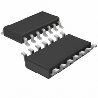
LT1684CS Linear Technology, LT1684CS Datasheet - Page 8

LT1684CS
Manufacturer Part Number
LT1684CS
Description
IC RING TONE GENERATOR 14-SOIC
Manufacturer
Linear Technology
Datasheet
1.LT1684CN.pdf
(16 pages)
Specifications of LT1684CS
Function
Tone Generator
Number Of Circuits
1
Operating Temperature
0°C ~ 125°C
Mounting Type
Surface Mount
Package / Case
14-SOIC (3.9mm Width), 14-SOL
Lead Free Status / RoHS Status
Contains lead / RoHS non-compliant
Current - Supply
-
Voltage - Supply
-
Power (watts)
-
Interface
-
Available stocks
Company
Part Number
Manufacturer
Quantity
Price
Part Number:
LT1684CS
Manufacturer:
LINEAR/凌特
Quantity:
20 000
Part Number:
LT1684CS#PBF
Manufacturer:
LINEAR/凌特
Quantity:
20 000
Part Number:
LT1684CS#TRPBF
Manufacturer:
LINEAR/凌特
Quantity:
20 000
APPLICATIO S I FOR ATIO
LT1684
Encoded PWM Signal Input Basics
The LT1684 accepts a user-supplied PWM carrier that
represents the desired output ring tone signal. This PWM
input is normalized by the LT1684 such that ring tone
output amplitudes can be accurately encoded into the
PWM input.
The LT1684 accepts a differential input to maximize rejec-
tion of system transients and ground noise. If no differen-
tial signal is readily available from the PWM controller, a
simple inverter/buffer block can be used to create the
differential signal required.
Each differential input is internally connected through a 5k
series resistor to back-to-back isolation-base diodes. These
devices internally clamp the differential input signal to
range. The input comparator toggles with a differential
hysteresis equal to that of a standard diode forward
voltage (0.7V nominal). As such, the differential imped-
ance of the input remains high throughout the input
hysteresis region, then reduces to a nominal value of 10k
(7k minimum) as the input is overdriven beyond the
comparator input threshold. A minimum differential input
of 1.6V is specified to assure valid switching.
The PWM signal can be visualized in terms of instanta-
neous ring tone amplitude, normalized to the LT1684
amplitude reference. For a given desired output voltage
V
8
100mV greater than the input comparator hysteresis
OUTN
V
DC = [V
V
DC = PWM input duty cycle
OUTN
REF
, the input pulse train required follows the relation:
= 1.25V normalized peak voltage
= 2 • V
OUTN
/ (2 • V
REF
U
• (DC – 0.5), or
REF
U
)] + 0.5, where:
W
U
A 10% to 90% duty cycle range is a practical limit for a
10kHz input carrier. This corresponds to normalized sig-
nal amplitude of 1V. Duty cycles exceeding this range can
cause increased output signal distortion as signal energy
is lost due to finite rise and fall times becoming a signifi-
cant percentage of the signal pulses. The associated
reduction in the pulse energy manifests itself as a “soft
clipping” of the output signal resulting in an increase in
harmonic distortion.
The normalized PWM signal is amplified to the desired
output signal level by the active filter/amplifier stage.
Thus, dividing the desired peak output amplitude by the
peak normalized encoded amplitude (V
the required DC gain of the active filter.
System Considerations
Assuming use of a 10% to 90% maximum PWM range, the
peak normalized signal will be:
Thus, the DC gain of the output filter equals the desired
peak voltage of the output ring tone signal.
The frequency characteristics of the lowpass output filter
must reflect the allowable carrier ripple on the output
signal. For example, a 10kHz carrier system could use a
2-pole Butterworth lowpass with a cutoff frequency of
100Hz. This filter provides 40dB of input signal rejection
at 10kHz yielding 25mV
the output filter/amplifier was 100, the output ripple volt-
age would be riding on a 100V sine wave, and therefore
be about – 78dB relative to the output ring signal.
V
V
PWM
OUT
(pk) = V
(pk) = 0.8 • V
PWM
(pk) • Filter DC Gain
P-P
REF
output ripple. If the DC gain of
= 1.0V, and:
OUT
/V
OUTN
) yields


