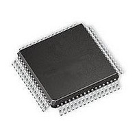
SI3232-BQ Silicon Laboratories Inc, SI3232-BQ Datasheet - Page 49

SI3232-BQ
Manufacturer Part Number
SI3232-BQ
Description
IC SLIC PROG DUAL-CH 64TQFP
Manufacturer
Silicon Laboratories Inc
Specifications of SI3232-BQ
Package / Case
*
Function
Subscriber Line Interface Concept (SLIC)
Interface
ISDN
Number Of Circuits
2
Voltage - Supply
3.13 V ~ 3.47 V
Current - Supply
28mA
Power (watts)
280mW
Operating Temperature
0°C ~ 70°C
Mounting Type
Surface Mount
Product
SLIC
Supply Voltage (min)
3.13 V
Supply Current
28 mA
Maximum Operating Temperature
+ 85 C
Minimum Operating Temperature
- 40 C
Mounting Style
SMD/SMT
Number Of Channels
2
Lead Free Status / RoHS Status
Contains lead / RoHS non-compliant
Available stocks
Company
Part Number
Manufacturer
Quantity
Price
Company:
Part Number:
SI3232-BQ
Manufacturer:
Silicon Laboratories Inc
Quantity:
10 000
The bits are defined in Table 29.
Si3232 RAM and Register Space
The Si3232 is a highly-programmable telephone
linecard solution that uses internal registers and RAM to
program operational parameters and modes. The
Register Summary and RAM Summary are compressed
listings for single-entry quick reference. The Register
Descriptions and RAM Descriptions give detailed
information of each register or RAM location’s bits.
All RAM locations are cleared upon a hardware reset.
All RAM locations that are listed as “INIT” must be
initialized to a meaningful value for proper functionality.
Bit 4 of the MSTRSTAT register indicates the clearing
process is finished. This bit should be checked before
initializing the RAM space.
Accessing register and RAM space is performed
through the SPI. Register space is accessed by using
the standard three-byte access as described in the next
section. Bit 5 of the control byte specifies register
access when set to a 1. All register space is comprised
of 8-bit data.
RAM Access by Pipeline
Ram space can be accessed by two different methods.
One method is a pipeline method that employs a 4-byte
access plus a RAM status check. The control byte for
the pipeline method has bit 6 cleared to 0 to indicate a
RAM access. The control byte is followed by the RAM
address byte, then the two data bytes.
3:0
7
6
5
4
REG/RAM Register/RAM Access.
Reserved
BRDCST Indicates a broadcast operation that is intended for all devices in the daisy chain. This is
CID[3:0]
R/W
only valid for write operations since it would cause contention on the SDO pin during a
read.
Read/Write Bit.
0 = Write operation.
1 = Read operation.
0 = RAM access.
1 = Register access.
This field indicates the channel that is targeted by the operation. The 4-bit channel value is
provided LSB first. The devices reside on the daisy chain such that device 0 is nearest to
the controller, and device 15 is furthest down the SDI/SDU_THRU chain. (See Figure 26.)
As the CID information propagates down the daisy chain, each channel decrements the
CID by 1. The SDI nodes between devices will reflect a decrement of 2 per device since
each device contains two channels. The device receiving a value of 0 in the CID field will
respond to the SPI transaction. (See Figure 27.) If a broadcast to all devices connected to
the chain is requested, the CID will not decrement. In this case, the same 8-bit or 16-bit
data is presented to all channels regardless of the CID values.
Table 29. SPI Control Interface
Preliminary Rev. 0.95
Reading RAM in the pipeline method requires “priming”
the data. First, check for register RAMSTAT, bit 0, to
indicate the previous access is complete and RAM is
ready (0). Then, perform the 4-byte RAM access. The
first read will yield unusable data. The data read on the
subsequent read access is the data for the previous
address read. A final address read yields the last
previously-requested data. The RAM-ready information
(RAMSTAT) must be read before every RAM access.
To write a RAM location, check for register RAMSTAT,
bit 0, to indicate the previous access is complete and
RAM is ready (0). Then, write the RAM address and
data in the 4-byte method. A write to RAM location
requires “priming” the data with subsequent accesses.
RAM Access by Register
An alternative method to access RAM space utilizes
three registers in sequence and monitors RAMSTAT
register, bit 0. These three registers are RAMADDR,
RAMDATLO, and RAMDATHI.
To read a RAM location in the Si3232, check for register
RAMSTAT (bit 0) to indicate the previous access is
complete and RAM is ready (0). Then, write the RAM
address to RAMADDR. Wait until RAMSTAT (bit 0) is a
1; then, the 16 bits of data can be read from the
RAMDATLO and RAMDATHI registers.
To write a RAM location in the Si3232, check for register
RAMSTAT (bit 0) to indicate the previous access is
completed and RAM is ready (0); then, write the 16 bits
Si3232
49


