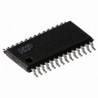
SC16IS752IPW,112 NXP Semiconductors, SC16IS752IPW,112 Datasheet - Page 23

SC16IS752IPW,112
Manufacturer Part Number
SC16IS752IPW,112
Description
IC UART DUAL 12C/SPI 28TSSOP
Manufacturer
NXP Semiconductors
Type
IrDA or RS- 232 or RS- 485r
Datasheet
1.SC16IS752IBS151.pdf
(59 pages)
Specifications of SC16IS752IPW,112
Number Of Channels
2, DUART
Package / Case
28-TSSOP (0.173", 4.40mm Width)
Features
Low Current
Fifo's
64 Byte
Protocol
RS232, RS485
Voltage - Supply
2.5V, 3.3V
With Auto Flow Control
Yes
With Irda Encoder/decoder
Yes
With False Start Bit Detection
Yes
With Modem Control
Yes
Mounting Type
Surface Mount
Data Rate
5 Mbps
Supply Voltage (max)
3.6 V
Supply Voltage (min)
2.3 V
Supply Current
6 mA
Maximum Operating Temperature
+ 95 C
Minimum Operating Temperature
- 40 C
Mounting Style
SMD/SMT
Operating Supply Voltage
2.5 V or 3.3 V
Lead Free Status / RoHS Status
Lead free / RoHS Compliant
For Use With
568-4000 - DEMO BOARD SPI/I2C TO DUAL UART568-3510 - DEMO BOARD SPI/I2C TO UART
Lead Free Status / Rohs Status
Lead free / RoHS Compliant
Other names
568-4016-5
935279292112
SC16IS752IPW
SC16IS752IPW
935279292112
SC16IS752IPW
SC16IS752IPW
NXP Semiconductors
SC16IS752_SC16IS762_7
Product data sheet
8.4 FIFO Control Register (FCR)
Table 11.
[1]
This is a write-only register that is used for enabling the FIFOs, clearing the FIFOs, setting
transmitter and receiver trigger levels.
Table 12.
[1]
Bit
1
0
Bit
7:6
5:4
3
2
1
0
IER[7:4] can only be modified if EFR[4] is set, that is, EFR[4] is a write enable. Re-enabling IER[1] will not
cause a new interrupt if the THR is below the threshold.
FIFO reset logic requires at least two XTAL1 clocks, therefore, they cannot be reset without the presence of
the XTAL1 clock.
Symbol
IER[1]
IER[0]
Symbol
FCR[7] (MSB),
FCR[6] (LSB)
FCR[5] (MSB),
FCR[4] (LSB)
FCR[3]
FCR[2]
FCR[1]
FCR[0]
Interrupt Enable Register bits description
FIFO Control Register bits description
[1]
[1]
Description
Transmit Holding Register interrupt.
Receive Holding Register interrupt.
logic 0 = disable the THR interrupt (normal default condition)
logic 1 = enable the THR interrupt
logic 0 = disable the RHR interrupt (normal default condition)
logic 1 = enable the RHR interrupt
Dual UART with I
Rev. 07 — 19 May 2008
Description
RX trigger. Sets the trigger level for the RX FIFO.
TX trigger. Sets the trigger level for the TX FIFO.
FCR[5:4] can only be modified and enabled when EFR[4] is set. This is
because the transmit trigger level is regarded as an enhanced function.
reserved
Reset TX FIFO.
Reset RX FIFO
FIFO enable
00 = 8 characters
01 = 16 characters
10 = 56 characters
11 = 60 characters
00 = 8 spaces
01 = 16 spaces
10 = 32 spaces
11 = 56 spaces
logic 0 = no FIFO transmit reset (normal default condition)
logic 1 = clears the contents of the transmit FIFO and resets the FIFO
level logic (the Transmit Shift Register is not cleared or altered). This
bit will return to a logic 0 after clearing the FIFO.
logic 0 = no FIFO receive reset (normal default condition)
logic 1 = clears the contents of the receive FIFO and resets the FIFO
level logic (the Receive Shift Register is not cleared or altered). This
bit will return to a logic 0 after clearing the FIFO.
logic 0 = disable the transmit and receive FIFO (normal default
condition)
logic 1 = enable the transmit and receive FIFO
Table 12
2
SC16IS752/SC16IS762
C-bus/SPI interface, 64-byte FIFOs, IrDA SIR
shows FIFO Control Register bit settings.
…continued
© NXP B.V. 2008. All rights reserved.
23 of 59


