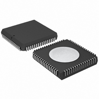
SC16C654BIA68,512 NXP Semiconductors, SC16C654BIA68,512 Datasheet - Page 31

SC16C654BIA68,512
Manufacturer Part Number
SC16C654BIA68,512
Description
ID QUAD UART 64BYTE 68PLCC
Manufacturer
NXP Semiconductors
Datasheet
1.SC16C654BIBS528.pdf
(58 pages)
Specifications of SC16C654BIA68,512
Features
False-start Bit Detection
Number Of Channels
4, QUART
Fifo's
64 Byte
Voltage - Supply
2.5V, 3.3V, 5V
With Auto Flow Control
Yes
With Irda Encoder/decoder
Yes
With False Start Bit Detection
Yes
With Modem Control
Yes
With Cmos
Yes
Mounting Type
Surface Mount
Package / Case
68-LCC (J-Lead)
Transmit Fifo
64Byte
Receive Fifo
64Byte
Transmitter And Receiver Fifo Counter
Yes
Data Rate
5Mbps
Package Type
PLCC
Operating Supply Voltage (max)
5.5V
Mounting
Surface Mount
Operating Temperature (min)
-40C
Operating Temperature (max)
85C
Operating Temperature Classification
Industrial
Lead Free Status / RoHS Status
Lead free / RoHS Compliant
Other names
935274935512
SC16C654BIA68
SC16C654BIA68
SC16C654BIA68
SC16C654BIA68
Available stocks
Company
Part Number
Manufacturer
Quantity
Price
Company:
Part Number:
SC16C654BIA68,512
Manufacturer:
NXP Semiconductors
Quantity:
10 000
Philips Semiconductors
9397 750 14965
Product data sheet
7.6 Modem Control Register (MCR)
Table 16:
Table 17:
Table 18:
This register controls the interface with the modem or a peripheral device.
Table 19:
LCR[5]
X
0
0
1
1
LCR[2]
0
1
1
LCR[1]
0
0
1
1
Bit
7
6
5
Symbol
MCR[7]
MCR[6]
MCR[5]
LCR[5] parity selection
LCR[2] stop bit length
LCR[1:0] word length
Modem Control Register bits description
LCR[4]
X
0
1
0
1
Word length
5, 6, 7, 8
5
6, 7, 8
LCR[0]
0
1
0
1
Description
Clock select.
IR enable.
Xon Any.
5 V, 3.3 V and 2.5 V quad UART, 5 Mbit/s (max.) with 64-byte FIFOs
logic 0 = divide-by-1. The input clock (crystal or external) is divided by 16
and then presented to the Programmable Baud Rate Generator (BGR)
without further modification, that is, divide-by-1. (normal default condition).
logic 1 = divide-by-4. The divide-by-1 clock described in MCR[7] = a logic 0,
if further divided by four. Also see
generator”.
logic 0 = enable the standard modem receive and transmit input/output
interface (normal default condition)
logic 1 = enable infrared IrDA receive and transmit inputs/outputs. While in
this mode, the TX/RX output/inputs are routed to the infrared
encoder/decoder. The data input and output levels will conform to the IrDA
infrared interface requirement. As such, while in this mode, the infrared TX
output will be a logic 0 during idle data conditions.
logic 0 = disable Xon Any function (for 16C554 compatibility) (normal default
condition)
logic 1 = enable Xon Any function. In this mode, any RX character received
will enable Xon
Rev. 02 — 20 June 2005
LCR[3]
0
1
1
1
1
Word length
5
6
7
8
Stop bit length (bit times)
1
1
2
1
2
Parity selection
no parity
odd parity
even parity
forced parity ‘1’
forced parity ‘0’
SC16C654B/654DB
Section 6.9 “Programmable baud rate
© Koninklijke Philips Electronics N.V. 2005. All rights reserved.
31 of 58


