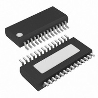
MAX3140CEI+T Maxim Integrated Products, MAX3140CEI+T Datasheet - Page 2

MAX3140CEI+T
Manufacturer Part Number
MAX3140CEI+T
Description
IC UART W/RS485 28-QSOP
Manufacturer
Maxim Integrated Products
Datasheet
1.MAX3140CEIT.pdf
(36 pages)
Specifications of MAX3140CEI+T
Features
Transceiver
Fifo's
8 Byte
Protocol
RS232, RS485
Voltage - Supply
4.75 V ~ 5.25 V
With Irda Encoder/decoder
Yes
With False Start Bit Detection
Yes
With Cmos
Yes
Mounting Type
Surface Mount
Package / Case
28-QSOP
Lead Free Status / RoHS Status
Lead free / RoHS Compliant
ABSOLUTE MAXIMUM RATINGS
V
Input Voltage to GND (CS, SHDN, X1, CTS, RX, DIN, SCLK,
Output Voltage to GND
Driver Output Voltage (Y, Z) ...............................................±13V
Receiver Input Voltage, Half Duplex (Y, Z)......................... ±13V
Receiver Input Voltage, Full Duplex (A, B) .........................±25V
TX, RTS Output Current ...................................................100mA
SPI/MICROWIRE-Compatible UART with Integrated
True Fail-Safe RS-485/RS-422 Transceivers
ELECTRICAL CHARACTERISTICS
(V
are measured with V
Stresses beyond those listed under “Absolute Maximum Ratings” may cause permanent damage to the device. These are stress ratings only, and functional
operation of the device at these or any other conditions beyond those indicated in the operational sections of the specifications is not implied. Exposure to
absolute maximum rating conditions for extended periods may affect device reliability.
2
POWER SUPPLY
UART OSCILLATOR INPUT (X1)
UART LOGIC INPUTS (DIN, SCLK, CS, SHDN, CTS, RX)
UART OUTPUTS (DOUT, TX, RTS)
CC
Supply Voltage
Supply Current
Supply Current with Only UART
Shut Down
Supply Current with Both
RS-485 Transceiver and UART
Shut Down
Input High Voltage
Input Low Voltage
Input Current
Input Capacitance
Input High Voltage
Input Low Voltage
Input Hysteresis
Input Leakage Current
Input Capacitance
Output High Voltage
Output Low Voltage
Output Leakage
Output Capacitance
RE, DE, H/F, SRL, TXP, RXP, Dl) .............-0.3V to (V
DOUT, RTS, TX, X2, RO...........................-0.3V to (V
IRQ ........................................................................-0.3V to +6V
CC
_______________________________________________________________________________________
to GND ..........................................................................+6V
= +5V ±5%, DE = V
PARAMETER
CC
= +5V, UART configured for 9600 baud, T
CC
, RE = GND, SHDN = V
SYMBOL
I
I
CC
CC
V
(FULL)
C
UART
I
I
V
V
C
HYST2
C
V
V
V
LKG1
LKG2
V
V
I
I
OUT1
OH1
SHDN
SHDN
IN1
OL1
CC
IH1
IH2
CC
IL1
IN1
IL2
IN2
SHDN = V
SHDNi bit = 0,
no load
SHDN = GND or SHDNi bit = 1
SHDN = GND or SHDNi bit = 1;
DE = GND; RE = V
V
I
I
I
I
CS = V
SOURCE
SOURCE
SINK
SINK
X1
CC
= 0 or V
CC
CC
= 4mA; DOUT, RTS
= 25mA; TX only
, f
CC
+ 0.3V)
+ 0.3V)
XTL
= 5mA; DOUT, RTS
= 10mA; TX only
; D
CC
CC
OUT
= 1.8432MHz, T
;
CONDITIONS
only
A
CC
SRL = V
SRL = GND
or open
= +25°C.) (Note 1)
X2, DOUT, IRQ Short-Circuit Duration
Continuous Power Dissipation (T
Operating Temperature Ranges
Storage Temperature Range .............................-65°C to +150°C
Lead Temperature (soldering, 10sec) .............................+300°C
Soldering Temperature (reflow) .......................................+260°C
(to V
28-pin QSOP (derate 10.8mW/°C above +70°C)..........860mW
MAX3140CEI .......................................................0°C to +70°C
MAX3140EEI ....................................................-40°C to +85°C
SHDNi bit = 0
SHDNi bit = 1
CC
CC
A
= T
or GND) ......................................................Continuous
MIN
DE = V
DE = GND
DE = V
DE = GND
to T
MAX
CC
CC
, unless otherwise noted. Typical values
V
V
0.7V
0.7V
CC
CC
4.75
MIN
CC
CC
- 0.5
- 0.5
A
= +70°C)
TYP
0.64
0.74
0.69
0.47
250
0.7
5
5
5
0.2V
0.3V
MAX
5.25
1.9
1.6
1.8
0.4
0.9
20
25
±1
±1
2
1
2
CC
CC
UNITS
mA
mA
mV
µA
µA
µA
µA
pF
pF
pF
V
V
V
V
V
V
V


