LM4873LQX National Semiconductor, LM4873LQX Datasheet - Page 5
LM4873LQX
Manufacturer Part Number
LM4873LQX
Description
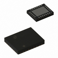
IC AMP AUDIO PWR 3W STER 24LLP
Manufacturer
National Semiconductor
Series
Boomer®r
Type
Class ABr
Datasheet
1.LM4873MTEXNOPB.pdf
(25 pages)
Specifications of LM4873LQX
Output Type
2-Channel (Stereo) with Stereo Headphones
Max Output Power X Channels @ Load
3W x 2 @ 3 Ohm; 440mW x 2 @ 8 Ohm
Voltage - Supply
2 V ~ 5.5 V
Features
Depop, Input Multiplexer, Shutdown, Thermal Protection
Mounting Type
Surface Mount
Package / Case
24-LLP
Lead Free Status / RoHS Status
Lead free / RoHS Compliant
Other names
*LM4873LQX
Available stocks
Company
Part Number
Manufacturer
Quantity
Price
Company:

Part Number:
LM4873LQX
Manufacturer:
ROHM
Quantity:
2 029


THD+N
PSRR
X
SNR
V
P
THD+N
PSRR
X
SNR
Symbol
Symbol
TALK
OS
O
TALK
Electrical Characteristics for Bridged-Mode Operation
The following specifications apply for V
Electrical Characteristics for Single-Ended Operation
Note 3: Absolute Maximum Ratings indicate limits beyond which damage to the device may occur. Operating Ratings indicate conditions for which the device is
functional, but do not guarantee specific performance limits. Electrical Characteristics state DC and AC electrical specifications under particular test conditions which
guarantee specific performance limits. This assumes that the device operates within the Operating Ratings. Specifications are not guaranteed for parameters where
no limit is given. The typical value however, is a good indication of device performance.
Note 4: The maximum power dissipation must be derated at elevated temperatures and is dictated by T
allowable power dissipation is P
Information section or the Absolute Maximum Ratings section.
Note 5: Human body model, 100 pF discharged through a 1.5 kΩ resistor.
Note 6: Machine model, 220 pF–240 pF discharged through all pins.
Note 7: The given θ
Note 8: The given θ
Note 9: The given θ
Note 10: The given θ
Note 11: The given θ
Note 12: The given θ
Note 13: The given θ
Note 14: The θ
Note 15: All voltages are measured with respect to the ground (GND) pins, unless otherwise specified.
Note 16: Typicals are specified at 25˚C and represent the parametric norm.
Note 17: Datasheet min/max specification limits are guaranteed by design, test, or statistical analysis.
The following specifications apply for V
Output Offset Voltage
Output Power
Total Harmonic Distortion+Noise
Power Supply Rejection Ratio
Channel Separation
Signal To Noise Ratio
Total Harmonic Distortion+Noise
Power Supply Rejection Ratio
Channel Separation
Signal To Noise Ratio
JA
is specified for an LM4873 packaged in a BLA20AAB or TLA20AAA with their four ground connections soldered to a 3in
JA
JA
JA
JA
JA
JA
JA
is for an LM4873 packaged in an MXA20A with the Exposed-DAP soldered to an exposed 2in
is for an LM4873 packaged in an MXA20A with the Exposed-DAP soldered to an exposed 1in
is for an LM4873 packaged in an MXA20A with the Exposed-DAP not soldered to printed circuit board copper.
is for an LM4873 packaged in an MXA28A with the Exposed-DAP soldered to an exposed 2in
is for an LM4873 packaged in an MXA28A with the Exposed-DAP soldered to an exposed 1in
is for an LM4873 packaged in an MXA28A with the Exposed-DAP not soldered to printed circuit board copper.
is for an LM4873 packaged in an LQA24A with the Exposed-DAP soldered to an exposed 2in
Parameter
Parameter
DMAX
= (T
JMAX
− T
DD
DD
= 5V unless otherwise specified. Limits apply for T
A
= 5V unless otherwise specified. Limits apply for T
V
THD+N = 0.5%, f = 1 kHz, R
THD+N = 1%, f = 1 kHz, R
THD+N = 10%, f = 1 kHz, R
A
R
C
f = 1kHz
f = 1kHz, C
V
)/θ
THD+N = 10%, f = 1kHz (Note 20)
THD+N = 1%, f = 1kHz, R
20Hz ≤ f ≤ 20kHz, A
V
C
f = 1kHz, C
V
IN
V
DD
L
B
JA
DD
B
DD
= −1, P
= 32Ω
. For the LM4873, T
= 1.0µF, V
= 0V
= 1.0µF
= 5V, P
LM4873MTE-1, R
LM4873LQ, R
LM4873MTE-1, R
LM4873LQ, R
LM4873, R
LM4873MTE-1, R
LM4873LQ, R
LM4873, R
= 5V, V
= 5V, P
O
B
B
O
= 75mW, 20Hz ≤ f ≤ 20kHz,
RIPPLE
O
= 1.0µF
RIPPLE
= 1.0µF
= 340mW, R
= 1.1W, R
L
L
= 8Ω
= 8Ω, P
Conditions
Conditions
L
L
L
5
JMAX
= 200mV
= 3Ω
= 4Ω
= 4Ω, P
VD
= 200mV
L
L
L
= 2
= 150˚C. For the θ
= 3Ω
= 4Ω
= 4Ω, P
L
O
L
= 8Ω
L
L
= 1W
O
L
= 8Ω
= 32Ω
= 8Ω
L
RMS
= 8Ω
= 2W
= 32Ω
RMS
O
, R
= 2W
,
L
JMAX
= 8Ω,
JA
, θ
s for different packages, please see the Application
JA
, and the ambient temperature T
(Notes 3, 15)
(Notes 3, 15) (Continued)
2
2
A
2
A
2
2
= 25˚C.
area of 1oz printed circuit board copper.
area of 1oz printed circuit board copper.
(Note 16) (Note 17)
= 25˚C.
area of 1oz printed circuit board copper.
area of 1oz printed circuit board copper.
Typical
area of 1oz printed circuit board copper.
(Note 16)
Typical
0.34
3.0
3.0
2.6
2.6
1.5
0.3
0.3
67
80
97
340
440
0.2
85
52
60
94
5
LM4873
LM4873
(Note 17)
Limit
2
Limit
, 1oz copper plane.
50
75
A
. The maximum
www.national.com
(Limits)
mV (max)
mW (min)
Units
(Limits)
dB
dB
dB
W
W
W
W
W
W
%
Units
mW
mW
dB
dB
dB
%
Related parts for LM4873LQX
Image
Part Number
Description
Manufacturer
Datasheet
Request
R

Part Number:
Description:
National Semiconductor [8-Bit D/A Converter]
Manufacturer:
National Semiconductor
Datasheet:
Part Number:
Description:
National Semiconductor [Media Coprocessor]
Manufacturer:
National Semiconductor
Datasheet:
Part Number:
Description:
Digitally Controlled Tone and Volume Circuit with Stereo Audio Power Amplifier, Microphone Preamp Stage and National 3D Sound
Manufacturer:
National Semiconductor
Datasheet:
Part Number:
Description:
Digitally Controlled Tone and Volume Circuit with Stereo Audio Power Amplifier, Microphone Preamp Stage and National 3D Sound
Manufacturer:
National Semiconductor
Datasheet:
Part Number:
Description:
AC97 Rev 2 Codec with Sample Rate Conversion and National 3D Sound
Manufacturer:
National Semiconductor
Part Number:
Description:
Manufacturer:
National Semiconductor
Datasheet:
Part Number:
Description:
Manufacturer:
National Semiconductor
Datasheet:
Part Number:
Description:
General Purpose, Low Voltage, Low Power, Rail-to-Rail Output Operational Amplifiers
Manufacturer:
National Semiconductor
Datasheet:
Part Number:
Description:
8-bit 20 MSPS flash A/D converter.
Manufacturer:
National Semiconductor
Datasheet:
Part Number:
Description:
Low Noise Quad Operational Amplifier
Manufacturer:
National Semiconductor
Datasheet:
Part Number:
Description:
Quad Differential Line Receivers
Manufacturer:
National Semiconductor
Datasheet:
Part Number:
Description:
Quad High Speed Trapezoidal? Bus Transceiver
Manufacturer:
National Semiconductor
Datasheet:
Part Number:
Description:
Dual Line Receiver
Manufacturer:
National Semiconductor
Datasheet:
Part Number:
Description:
TTL to 10k ECL Level Translator with Latch
Manufacturer:
National Semiconductor
Datasheet: