NCP2892AFCT2G ON Semiconductor, NCP2892AFCT2G Datasheet
NCP2892AFCT2G
Specifications of NCP2892AFCT2G
Available stocks


Related parts for NCP2892AFCT2G

NCP2892AFCT2G Summary of contents
Page 1
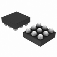
... PDAs • Wireless Phones *For additional information on our Pb−Free strategy and soldering details, please download the ON Semiconductor Soldering and Mounting Techniques Reference Manual, SOLDERRM/D. © Semiconductor Components Industries, LLC, 2006 September, 2006 − Rev. 3 http://onsemi.com 9−Pin Flip−Chip CSP ...
Page 2
Ci Ri INM AUDIO INPUT INP BYPASS bypass SHUTDOWN VIH VIL Figure 1. Typical Audio Amplifier Application Circuit with Single Ended Input INM AUDIO INP INPUT ...
Page 3
PIN DESCRIPTION Pin Type Symbol A1 I INM A2 O OUTA A3 I INP B1 I VM_P BYPASS C2 O OUTB C3 I SHUTDOWN MAXIMUM RATINGS (Note 1) Rating Supply Voltage ...
Page 4
ELECTRICAL CHARACTERISTICS Limits apply for T Characteristic Supply Quiescent Current Common Mode Voltage Shutdown Current Shutdown Voltage High Shutdown Voltage Low Turning On Time (Note 9) Turning Off Time Output Impedance in Shutdown Mode NCP2892A NCP2892B Output Swing NCP2892A Output ...
Page 5
ELECTRICAL CHARACTERISTICS Limits apply for T Characteristic Thermal Shutdown Temperature (Note 10) Total Harmonic Distortion 7. Min/Max limits are guaranteed by design, test or statistical analysis. 8. This parameter is guaranteed but not tested in production in case of a ...
Page 6
TYPICAL PERFORMANCE CHARACTERISTICS 2.5 V NCP2892A kHz 0.1 0.01 0.001 0 50 100 150 200 250 P , POWER OUT (mW) out Figure ...
Page 7
TYPICAL PERFORMANCE CHARACTERISTICS 1700 = 1500 kHz 1300 V THD+N < 10% 1100 900 700 500 300 100 2.5 3.0 3.5 4.0 POWER SUPPLY (V) Figure 9. Output Power versus ...
Page 8
TYPICAL PERFORMANCE CHARACTERISTICS − 3 − 200 mV ripple pk−pk Input to Gnd − bypass −40 −50 −60 −70 −80 10 100 1000 FREQUENCY (Hz) ...
Page 9
TYPICAL PERFORMANCE CHARACTERISTICS 180 160 140 120 100 400 800 1200 C (nF) bypass Figure 21. T versus C ON bypass T = +255C ...
Page 10
TYPICAL PERFORMANCE CHARACTERISTICS 0.4 0. 0.3 0.25 0 0. kHz 0.05 THD + N < 0. 0.05 0.1 0.15 ...
Page 11
TYPICAL PERFORMANCE CHARACTERISTICS Ch1 = OUTA Ch2 = OUTB Ch3 = Shutdown Math1 = Ch1−Ch2: Differential Signal seen by the Load Figure 30. Zero Pop Noise Turn On Sequence with Differential Input to Ground 100 nF ...
Page 12
Detailed Description The NCP2892 audio amplifier can operate under 2.6 V until 5.5 V power supply. With less than 1% THD+N, B version can deliver up to 1.2 W rms output power to an 8.0 W load (V = 5.0 ...
Page 13
Gain−Setting Resistor Selection ( and R set the closed−loop gain of the amplifier order to optimize device and system performance, the NCP2892 should be used in low gain configurations. The low gain configuration minimizes THD ...
Page 14
NCP2892 Series Silkscreen Layer Figure 35. Demonstration Board for 9−Pin Flip−Chip CSP Device − PCB Layers http://onsemi.com 14 ...
Page 15
... Tape and Reel Packaging Specifications Brochure, BRD8011/D. NOTE: The NCP2892AFCT2G version requires a lead−free solder paste and should not be used with a SnPb solder paste. NCP2892 Series ...
Page 16
... SCILLC is an Equal Opportunity/Affirmative Action Employer. This literature is subject to all applicable copyright laws and is not for resale in any manner. PUBLICATION ORDERING INFORMATION LITERATURE FULFILLMENT: Literature Distribution Center for ON Semiconductor P.O. Box 5163, Denver, Colorado 80217 USA Phone: 303−675−2175 or 800−344−3860 Toll Free USA/Canada Fax: 303− ...