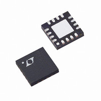
LTC6400IUD-26#PBF Linear Technology, LTC6400IUD-26#PBF Datasheet

LTC6400IUD-26#PBF
Specifications of LTC6400IUD-26#PBF
Related parts for LTC6400IUD-26#PBF
LTC6400IUD-26#PBF Summary of contents
Page 1
... The LTC6400-26 is packaged in a compact 16-lead 3mm × 3mm QFN package and operates over the –40°C to 85°C temperature range. L, LT, LTC and LTM are registered trademarks of Linear Technology Corporation. All other trademarks are the property of their respective owners. 3.3V 33pF 15Ω ...
Page 2
... TAPE AND REEL LTC6400CUD-26#PBF LTC6400CUD-26#TRPBF LCCX LTC6400IUD-26#PBF LTC6400IUD-26#TRPBF LCCX Consult LTC Marketing for parts specifi ed with wider operating temperature ranges. *The temperature grade is identifi label on the shipping container. Consult LTC Marketing for information on non-standard lead based fi nish parts. ...
Page 3
DC ELECTRICAL CHARACTERISTICS temperature range, otherwise specifi cations are at T otherwise noted. SYMBOL PARAMETER Input/Output Characteristic (+IN, –IN, +OUT, –OUT, +OUTF, –OUTF) G Gain DIFF TC Gain Temperature Drift GAIN V Output Swing Low SWINGMIN V Output Swing High ...
Page 4
LTC6400-26 AC ELECTRICAL CHARACTERISTICS ENABLE = 0V unless otherwise noted. L SYMBOL PARAMETER –3dBBW –3dB Bandwidth 0.5dBBW Bandwidth for 0.5dB Flatness 0.1dBBW Bandwidth for 0.1dB Flatness 1/f 1/f Noise Corner SR Slew Rate t 1% Settling Time S1% ...
Page 5
AC ELECTRICAL CHARACTERISTICS ENABLE = 0V unless otherwise noted. L SYMBOL PARAMETER P 1dB Compression Point 1dB,140M NF Noise Figure 140M e Input Referred Voltage Noise Density N,140M e Output Referred Voltage Noise Density ON,140M 240MHz Input Signal ...
Page 6
LTC6400-26 TYPICAL PERFORMANCE CHARACTERISTICS Frequency Response TEST CIRCUIT 100 FREQUENCY (MHz) S21 Phase and Group Delay vs Frequency 0 –50 GROUP DELAY –100 –150 –200 0 200 400 600 FREQUENCY (MHz) ...
Page 7
TYPICAL PERFORMANCE CHARACTERISTICS Noise Figure and Input Referred Noise Voltage vs Frequency NOISE FIGURE 100 FREQUENCY (MHz) Large Signal Transient Response 2 87.5Ω PER OUTPUT L TEST CIRCUIT B 2.0 ...
Page 8
LTC6400-26 TYPICAL PERFORMANCE CHARACTERISTICS Third Order Intermodulation Distortion vs Frequency –40 DIFFERENTIAL INPUT COMPOSITE OUT P-P –50 –60 –70 –80 –90 –100 200Ω L –110 0 50 100 150 200 250 FREQUENCY ...
Page 9
PIN FUNCTIONS + V (Pins 1, 3, 10): Positive Power Supply (Normally tied 3.3V). All three pins must be tied to the same voltage. Bypass each pin with 1000pF and 0.1μF capaci- tors as close to the ...
Page 10
LTC6400-26 APPLICATIONS INFORMATION Circuit Operation The LTC6400- low noise and low distortion fully differential op amp/ADC driver with: • Operation from DC to 1.9GHz –3dB bandwidth • Fixed gain of 20V/V (26dB) • Differential input impedance 50Ω • ...
Page 11
APPLICATIONS INFORMATION R S 0.1μF 50Ω 25Ω 500Ω – 150Ω IN+ OUT– 14 +IN 15 –IN IN– OUT+ 0.1μF 25Ω 500Ω 16 –IN 37.4Ω Figure 3. Input Termination for Single-Ended 50Ω Input Impedance ...
Page 12
LTC6400-26 APPLICATIONS INFORMATION LTC6400-26 500Ω 25Ω 12.5Ω 13 +IN +OUT 50Ω IN+ OUT– +OUTF 14 +IN 1.7pF 50Ω 15 –IN IN– OUT+ –OUTF 500Ω 25Ω 12.5Ω 16 –IN –OUT 640026 F06 Figure 6. LTC6400-26 with 165MHz Output Bandpass Filter converted ...
Page 13
TYPICAL APPLICATION R2 (1) R6 0Ω (2) (2) + (1) 0dB –IN (2) R1 0Ω R19 1.5k TP5 V OCM R20 1k T3 R17 TCM 4:19 0Ω ...
Page 14
LTC6400-26 TYPICAL APPLICATIONS +IN 24.9Ω PORT 1 (50Ω) 0.1μF +IN 1/2 AGILENT –IN E5O71A –IN 24.9Ω PORT 2 (50Ω) 0.1μF 1000pF 14 Test Circuit B, 4-Port Analysis + V 1000pF 0.1μF V – + ENABLE BIAS ...
Page 15
... ON THE TOP AND BOTTOM OF PACKAGE Information furnished by Linear Technology Corporation is believed to be accurate and reliable. However, no responsibility is assumed for its use. Linear Technology Corporation makes no representa- tion that the interconnection of its circuits as described herein will not infringe on existing patent rights. UD Package 16-Lead Plastic QFN (3mm × ...
Page 16
... SNR = 82dB at 3V Supply, 4th Order Filter SNR = 82dB at 3V Supply, 4th Order Filter SNR = 76dB at 3V Supply, 4th Order Filter SNR = 76dB at 3V Supply, 4th Order Filter www.linear.com ● – 640026fa LT 1108 REV A • PRINTED IN USA © LINEAR TECHNOLOGY CORPORATION 2008 ...


