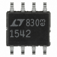
LTC1542CS8#PBF Linear Technology, LTC1542CS8#PBF Datasheet - Page 9

LTC1542CS8#PBF
Manufacturer Part Number
LTC1542CS8#PBF
Description
IC OPAMP/COMP/REF MICRPWR 8SOIC
Manufacturer
Linear Technology
Type
Amplifier, Comparator, Referencer
Datasheet
1.LTC1542CS8PBF.pdf
(12 pages)
Specifications of LTC1542CS8#PBF
Applications
General Purpose
Mounting Type
Surface Mount
Package / Case
8-SOIC (3.9mm Width)
Operating Temperature (min)
0C
Operating Temperature (max)
70C
Operating Temperature Classification
Commercial
Mounting
Surface Mount
Pin Count
8
Package Type
SOIC N
Lead Free Status / RoHS Status
Lead free / RoHS Compliant
Available stocks
Company
Part Number
Manufacturer
Quantity
Price
APPLICATIO S I FOR ATIO
The LTC1541/LTC1542 are a combination of a micropower
op amp, comparator and 1.2V ±1% reference (LTC1541)
in an 8-pin package. The LTC1541 has the negative input
of the comparator internally connected to the reference
output. The supply voltage range is from 2.5V to 12.6V for
single supply and ±1.25V to ±6.3V for dual supplies. The
supply current is a mere 5µA (typical) with a 5V single
supply.
Op Amp
The op amp is internally compensated to be unity-gain
stable, with typical GBW at 12kHz and slew rate of 8V/ms.
The output can drive a capacitive load of up to 1000pF and
swings from rail-to-rail. The input range is from the
negative rail to within 1.3V of the positive rail. The input
bias current is less than 1nA maximum at the extended
temperature range.
Comparator
The comparator has a high impedance differential input
stage with a common mode input range from the negative
rail to within 1.3V of the positive rail. The CMOS output
stage can swing from rail-to-rail and source up to 20mA
continuously. The output stage has been designed to
eliminate the power supply glitches that normally occur
when the output changes logic state. In addition, internal
hysteresis (±2.25mV) ensures clean output switching
even with slow moving input signals. The negative input is
internally connected to the reference for the LTC1541.
Reference
The internal bandgap reference has an output voltage of
1.2V ±1% over the industrial grade temperature range.
Figure 1. Damping the Reference Output
R1
C1
U
6
LTC1541
REF
U
×1
V
V
CC
SS
4
8
W
1541/42 F01
U
The output can source up to 2mA and sink up to 20µA with
a 5V supply. The output can drive a bypass capacitor of up
to 0.01µF without oscillation and by inserting a series
resistor, capacitance values up to 100µF can be used
(Figure 1). Figure 2 shows the resistor value required for
different capacitor values to achieve critical damping.
Bypassing the reference can help prevent false tripping of
the comparator by preventing glitches on V
load transients from disturbing the reference output volt-
age. Figures 3a and 3b show the bypass reference output
with a square wave applied to the V
damps the reference response. Note that the comparator
output doesn’t trip.
Op Amp Stability
Unlike other industry standard micropower CMOS op
amps, the op amp in the LTC1541/LTC1542 maintain
stability in unity-gain configuration while driving heavy
capacitive loads of up to 1000pF.
Although this family is primarily designed for low frequency
applications, good layout is extremely important. Low power,
high impedance circuits may increase the effects of board
leakage and stray capacitance. For example, the combina-
tion of a 10M resistance (from leakage between traces on a
contaminated, poorly designed PC board) and a 1pF stray
capacitance provides a pole at approximately 16kHz, which
is near the amplifier’s bandwidth. Board routing and layout
should minimize leakage and stray capacitance. In some
cases, stray capacitance may be unavoidable and it may be
necessary to add a small capacitor across the feedback
resistor to compensate (Figure 4); select the smallest
capacitor value that ensures stability.
Inputs
The input common mode range for both the op amp and
comparator is from the negative supply to within 1.3V of the
positive supply. The inputs can be taken more than 300mV
below the negative supply without damaging the device if
the current out of the pin is limited to less than 1mA. Unlike
bipolar input op amps and comparators, the outputs of the
CMOS LTC1541/LTC1542 will not reverse phase when the
inputs are taken above the common mode input range.
LTC1541/LTC1542
CC
pin while resistor R1
CC
or reference
15412fd
9


