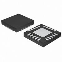
MAX3964AETP+ Maxim Integrated Products, MAX3964AETP+ Datasheet - Page 6

MAX3964AETP+
Manufacturer Part Number
MAX3964AETP+
Description
IC AMP LIMITING SGNL DET 20-TQFN
Manufacturer
Maxim Integrated Products
Type
Limiting Amplifierr
Datasheet
1.MAX3964AETP.pdf
(11 pages)
Specifications of MAX3964AETP+
Applications
Optical Networks
Mounting Type
Surface Mount
Package / Case
20-TQFN Exposed Pad
Operating Supply Voltage
5 V
Supply Current
22 mA
Operating Temperature Range
+ 85 C
Mounting Style
SMD/SMT
Number Of Channels
1
Power Dissipation
1349 mW
Lead Free Status / RoHS Status
Lead free / RoHS Compliant
+3.0V to +5.5V, 125Mbps to 266Mbps
Limiting Amplifiers with Loss-of-Signal Detector
The MAX3964A contains a series of limiting amplifiers
and power detectors, offset correction, data-squelch cir-
cuitry, and PECL output buffers for data and loss-of-sig-
nal (LOS) outputs. The MAX3968 provides PECL LOS
outputs with data outputs suitable for 266Mbps. Figure 1
shows a functional diagram of the MAX3964A/MAX3968.
A series of four limiting amplifiers provides gain of
approximately 65dB.
Each amplifier stage contains a full-wave logarithmic
detector (FWD), which indicates the RMS input signal
power. The FWD outputs are summed together at the
FILTER pin where the signal is filtered by an external
capacitor (CFILTER) connected between FILTER and
V
age, which is proportional to the input power in deci-
bels. When LOS+ is low, V
following equation:
where V
Figure 1. Functional Diagram
6
CC
C
FILTER
_______________________________________________________________________________________
. The FILTER signal generates the RSSI output volt-
IN+/IN-
FWD = FULL-WAVE DETECTOR
IN
V
CC
is measured in mV
FILTER
V
RSSI
(V) = 1.2V + 0.5log (V
MAX3964A
MAX3968
Detailed Description
V
FWD
CC
RSSI
LIMITER
P-P
Limiting Amplifiers
is approximated by the
.
FWD
Power Detector
REFERENCE
LIMITER
1.2V
IN
R1
INV
)
CZP
FWD
CORRECTION
OFFSET
R2
LIMITER
C
AZ
VTR
CZN
FWD
LIMITER
This relation translates to a 25mV increase in V
every 1dB increase in V
reduced approximately 120mV when LOS+ is asserted.
The data outputs (OUT+, OUT-) and the MAX3964A/
MAX3968 loss-of-signal outputs (LOS+, LOS-) are sup-
ply-referenced PECL outputs. Standard PECL termina-
tion at each output of 50Ω to (V
for best performance.
A low-frequency feedback loop around the limiting
amplifier improves receiver sensitivity and powerdetec-
tor accuracy. The offset-correction loop’s bandwidth is
determined by an external capacitor (CAZ) connected
between the CZP and CZN pins.
The offset correction is optimized for data streams with
a 50% duty cycle. A different average duty cycle
results in increased pulse-width distortion and loss of
sensitivity. The offset-correction circuitry is less sensi-
tive to variations of input duty cycle (for example, the
40% to 60% duty cycle encountered in 4B/5B coding)
when the input is less than 30mV
SUB
I
GND
LOS
COMPARATOR
I
O
IN
Input Offset Correction
(25mV/dB). The RSSI output is
CC
LOS+
V
CCO
P-P
- 2V) is recommended
.
PECL Outputs
OUT+/OUT-
SQUELCH
RSSI
LOS+/LOS-
RSSI
for


