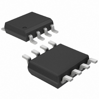
MAX953ESA+ Maxim Integrated Products, MAX953ESA+ Datasheet - Page 10

MAX953ESA+
Manufacturer Part Number
MAX953ESA+
Description
IC OP AMP SS LP 8-SOIC
Manufacturer
Maxim Integrated Products
Type
Amplifier, Comparatorr
Datasheet
1.MAX954ESA.pdf
(12 pages)
Specifications of MAX953ESA+
Applications
General Purpose
Mounting Type
Surface Mount
Package / Case
8-SOIC (3.9mm Width)
Lead Free Status / RoHS Status
Lead free / RoHS Compliant
6) Select the upper trip point V
7) Calculate R
Because low power requirements often demand high-
impedance circuits, effects from radiated noise are more
significant. Thus, traces between the op amp or com-
parator inputs and any resistor networks attached should
be kept as short as possible.
Internal crosstalk to the reference from the comparator
is package dependent. Typical values (V
45mV for the plastic DIP package and 32mV for the SO
package. Applications using the reference for the op
amp or external circuitry can eliminate this crosstalk by
using a simple RC lowpass filter, as shown in Figure 5.
Internal crosstalk to the op amp from the comparator is
package dependent, but not input-referred. Typical
values (V
and 280µV for the SO package.
Ultra-Low-Power, Single-Supply
Op Amp + Comparator + Reference
Figure 3. Compensation for Feedback-Node Capacitance
10
In the example, R
at 4.75V.
where R
R
_______________________________________________________________________________________
B
R
=
A
( )
DD
R
≈
AMPIN+
B
2
R
= 5V) are 4mV for the plastic DIP package
is 8.19kΩ, or approximately 8.2kΩ.
2
R1
B
V
V
S H
.
SHYST
( )
V
(
DD
V
REF
−
A
Input Noise Considerations
is again 24kΩ.
,
(
+
2pF to 10pF
for V
V
REF
V
R2
IHYST
SHYST
S(H)
+
) ( )( )
V
. Our example is set
IHSYT
R
>>
2
AMPOUT
R
)
(
V
DD
A
R
IHYST
Crosstalk
A
Reference
= 5V) are
Op Amp
+
R
2
)
Unlike other industry-standard micropower CMOS
op amps, the op amps in the MAX951–MAX954 main-
tain stability in their minimum gain configuration while
driving heavy capacitive loads, as demonstrated in the
MAX951/MAX953 Op Amp Percent Overshoot vs.
Capacitive Load graph in the Typical Operating
Characteristics.
Although this family is primarily designed for low-
frequency applications, good layout is extremely impor-
tant. Low-power, high-impedance circuits may increase
the effects of board leakage and stray capacitance. For
example, the combination of a 10MΩ resistance (from
leakage between traces on a contaminated, poorly
designed PC board) and a 1pF stray capacitance
provides a pole at approximately 16kHz, which is near
the amplifier’s bandwidth. Board routing and layout
should minimize leakage and stray capacitance. In
some cases, stray capacitance may be unavoidable
and it may be necessary to add a 2pF to 10pF capaci-
tor across the feedback resistor to compensate; select
the smallest capacitor value that ensures stability.
With 100mV overdrive, comparator propagation delay
is typically 6µs. The Typical Operating Characteristics
show propagation delay for various overdrive levels.
Supply current can increase when the op amp in the
MAX951–MAX954 is overdriven to the negative supply rail.
For example, when connecting the op amp as a compara-
tor and applying a -100mV input overdrive, supply current
rises by around 15µA and 32µA for supply voltages of
2.8V and 7V, respectively.
Figure 4. Low-Frequency Radio Receiver Application
ANTENNA
L1
330mH
L1 x C1 =
C1
390pF
Op Amp Stability and Board Layout
A
(2πf
1
C1
330pF
C
)
2
B
C1
20pF to
60pF
0.1µF
C
LAYOUT-SENSITIVE AREA,
METAL RFI SHIELDING ADVISED
5.1MΩ
MAX952
AMP
1MΩ
Input Overdrive
Considerations
100kΩ 1.2V
20kΩ
0.1µF
REF
V
CC
COMP
= 5V
10MΩ


