AD532KD/+ Analog Devices Inc, AD532KD/+ Datasheet - Page 10
AD532KD/+
Manufacturer Part Number
AD532KD/+
Description
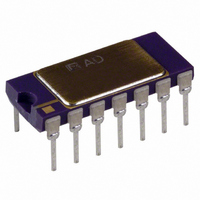
IC MULTIPLIER 10V 14-CDIP
Manufacturer
Analog Devices Inc
Datasheet
1.AD532JD.pdf
(16 pages)
Specifications of AD532KD/+
Rohs Status
RoHS non-compliant
Function
Analog Multiplier/Divider
Number Of Bits/stages
4-Quadrant
Package / Case
14-CDIP (0.300", 7.62mm)


FUNCTIONAL DESCRIPTION
The functional block diagram for the AD532 is shown in
Figure 1and the complete schematic in Figure 14. In the
multiplying and squaring modes, Z is connected to the output
to close the feedback around the output op amp. In the divide
mode, it is used as an input terminal.
The X and Y inputs are fed to high impedance differential
amplifiers featuring low distortion and good common-mode
rejection. The amplifier voltage offsets are actively laser trimmed to
AD532
COM
X
Y
X
Y
2
1
1
2
R2
R34
R18
R9
R1
Q1
Q3
Q5
R4
R3
Q6
Q4
Q2
R5
R10
R6
R32
Q28
Q7 Q8
Q9
Q11
R8
R12
R11
R13
Figure 14. Schematic Diagram
R14
R15
Q14 Q15
Q12
Q10
Rev. D | Page 10 of 16
R19
Q13
R16
R20
R21
Q19
Q16 Q17
Q18
R22
R24
zero during production. The product of the two inputs is resolved
in the multiplier cell using Gilbert’s linearized transconductance
technique. The cell is laser trimmed to obtain V
X
output impedance and make possible self-contained operation.
The residual output voltage offset can be zeroed at V
applications. Otherwise, the V
R23
2
Q20
)(Y
R25
1
− Y
C1
2
Q22
Q23
)/10 volts. The built-in op amp is used to obtain low
Q21
Q24
R26
Q26
R27
R31
Q27
Q25
R28
R30
R29
OS
R33
pin should be grounded.
+V
Z
V
OUTPUT
–V
OS
S
S
CAN
OUT
= (X
OS
in critical
1
−
Related parts for AD532KD/+
Image
Part Number
Description
Manufacturer
Datasheet
Request
R

Part Number:
Description:
±1.7g Dual-Axis IMEMS Accelerometer Evaluation Board
Manufacturer:
Analog Devices Inc
Datasheet:

Part Number:
Description:
Inertial Sensor Evaluation System
Manufacturer:
Analog Devices Inc
Datasheet:
Part Number:
Description:
Manufacturer:
Analog Devices Inc
Datasheet:
Part Number:
Description:
Manufacturer:
Analog Devices Inc
Datasheet:
Part Number:
Description:
Manufacturer:
Analog Devices Inc
Datasheet:
Part Number:
Description:
Manufacturer:
Analog Devices Inc
Datasheet:
Part Number:
Description:
Manufacturer:
Analog Devices Inc
Datasheet:
Part Number:
Description:
Manufacturer:
Analog Devices Inc
Datasheet:
Part Number:
Description:
Manufacturer:
Analog Devices Inc
Datasheet:
Part Number:
Description:
Manufacturer:
Analog Devices Inc
Datasheet:
Part Number:
Description:
Manufacturer:
Analog Devices Inc
Datasheet:
Part Number:
Description:
Manufacturer:
Analog Devices Inc
Datasheet:
Part Number:
Description:
Manufacturer:
Analog Devices Inc
Datasheet: