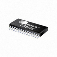
CS8406-CZZ Cirrus Logic Inc, CS8406-CZZ Datasheet - Page 13

CS8406-CZZ
Manufacturer Part Number
CS8406-CZZ
Description
IC XMITTER DGTL 192KHZ 28TSSOP
Manufacturer
Cirrus Logic Inc
Type
Digital Audio Interface Transmitterr
Datasheet
1.CS8406-CZZ.pdf
(42 pages)
Specifications of CS8406-CZZ
Package / Case
28-TSSOP
Applications
Automotive Audio
Mounting Type
Surface Mount
Operating Supply Voltage
3.3 V / 5.0 V
Operating Temperature Range
- 10 C to + 70 C
Mounting Style
SMD/SMT
Lead Free Status / RoHS Status
Lead free / RoHS Compliant
For Use With
598-1017 - BOARD EVAL FOR CS8416 RCVR
Lead Free Status / Rohs Status
Lead free / RoHS Compliant
Other names
598-1121-5
Available stocks
Company
Part Number
Manufacturer
Quantity
Price
Company:
Part Number:
CS8406-CZZ
Manufacturer:
CIRRUS
Quantity:
2 257
Company:
Part Number:
CS8406-CZZ
Manufacturer:
CIRRUS
Quantity:
10
Part Number:
CS8406-CZZ
Manufacturer:
CIRRUS
Quantity:
20 000
Company:
Part Number:
CS8406-CZZR
Manufacturer:
KINGBRIGHT
Quantity:
2 000
DS580F5
5. AES3 TRANSMITTER
The CS8406 includes an AES3 digital audio transmitter. A comprehensive buffering scheme provides write access
to the channel status and user data. This buffering scheme is described in
Data Buffer Management” on page
The AES3 transmitter encodes and transmits audio and digital data according to the AES3, IEC60958 (S/PDIF), and
EIAJ CP-1201 interface standards. Audio and control data are multiplexed together and bi-phase mark encoded.
The resulting bit stream is driven to an output connector either directly or through a transformer. The transmitter is
clocked from the clock input pin, OMCK. If OMCK is asynchronous to the data source, an interrupt bit (TSLIP) is
provided that will go high every time a data sample is dropped or repeated.
The channel status (C) and user (U) bits in the transmitted data stream are taken from storage areas within the
CS8406. The user can access the internal storage or configure the CS8406 to run in one of several automatic
modes.
of each automatic mode and describes methods of accessing the storage areas. The transmitted user bit data can
optionally be input through the U pin, under the control of a control port register bit.
Figures 8
5.1
5.2
5.3
“Appendix B: Channel Status and User Data Buffer Management” on page 39
TXN and TXP Drivers
The AES3 transmitter line drivers are low skew, low impedance, differential outputs capable of driving ca-
bles directly. Both drivers are set to ground during reset (RST = LOW), when no AES3 transmit clock is pro-
vided, and optionally under the control of a register bit. The CS8406 also allows immediate muting of the
AES3 transmitter audio data through a control register bit.
External components are used to terminate and isolate the external cable from the CS8406. These compo-
nents are detailed in
Mono Mode Operation
An alternate method for transmitting an AES3 192 kHz sample rate stream is Mono Mode. Mono Mode is
implemented by using the two sub-frames in a 96 kHz biphase encoded stream to carry consecutive sam-
ples of a single channel of a 192 kHz PCM stream (i.e. a mono signal). This allows older equipment, whose
AES3 transmitters and receivers are not rated for 192 kHz frame rate operation, to handle 192 kHz sample
rate information. In this Mono Mode, two AES3 cables and two CS8406's are needed for stereo data trans-
fer. The CS8406 is set to Mono Mode by the MMT control bit.
In Mono Mode, the input port will run at the audio sample rate (Fs), while the AES3 transmitter frame rate
will be at Fs/2. Consecutive left or right channel serial audio data samples may be selected for transmission
on the A and B sub-frames, and the channel status block transmitted is also selectable.
Using Mono Mode is only necessary if the incoming audio sample rate is already at 192 kHz and contains
both left and right audio data words. The “Mono Mode” AES3 output stream may also be achieved by keep-
ing the CS8406 in normal stereo mode, and placing consecutive audio samples in the left and right positions
in an incoming 96 kHz word rate data stream.
Transmitted Frame and Channel Status Boundary Timing
The TCBL pin is used to indicate the start of transmitted channel status block boundaries and may be an
input or an output.
In some applications, it may be necessary to control the precise timing of the transmitted AES3 frame
boundaries. This may be achieved in two ways:
and
9
show the C/U/V timing requirements.
“Appendix A: External AES3/SPDIF/IEC60958 Transmitter Components” on page
39.
Figure 9
shows the C/U/V timing requirements.
“Appendix B: Channel Status and User
provides detailed descriptions
CS8406
38.
13


