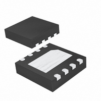
MAX9890BETA+T Maxim Integrated Products, MAX9890BETA+T Datasheet - Page 2

MAX9890BETA+T
Manufacturer Part Number
MAX9890BETA+T
Description
IC SUPPRESSOR CLICK-POP 8TDFN-EP
Manufacturer
Maxim Integrated Products
Type
Audio Suppressorr
Datasheet
1.MAX9890BETAT.pdf
(12 pages)
Specifications of MAX9890BETA+T
Applications
Cell Phone
Mounting Type
Surface Mount
Package / Case
8-TDFN Exposed Pad
Product
Audio Analog Processor
Operating Supply Voltage
2.7 V to 5.5 V
Supply Current
14 uA
Maximum Power Dissipation
1951 mW
Maximum Operating Temperature
+ 85 C
Mounting Style
SMD/SMT
Minimum Operating Temperature
- 40 C
Output Power
1.95W
Supply Voltage Range
2.7V To 5.5V
Operating Temperature Range
-40°C To +85°C
No. Of Pins
8
Digital Ic Case Style
TDFN
Filter Terminals
SMD
Rohs Compliant
Yes
Lead Free Status / RoHS Status
Lead free / RoHS Compliant
Other names
MAX9890BETA+T
MAX9890BETA+TTR
MAX9890BETA+TTR
ABSOLUTE MAXIMUM RATINGS
(All Voltages are Referenced to GND)
V
CEXT,
IN_ ..............................................................-0.3V to (V
Continuous Current (IN_, OUT_).....................................±150mA
Continuous Current (All Other Pins) .................................±20mA
Continuous Power Dissipation (T
Audio Click-Pop Suppressor
ELECTRICAL CHARACTERISTICS
(V
(Note 1)
Stresses beyond those listed under “Absolute Maximum Ratings” may cause permanent damage to the device. These are stress ratings only, and functional
operation of the device at these or any other conditions beyond those indicated in the operational sections of the specifications is not implied. Exposure to
absolute maximum rating conditions for extended periods may affect device reliability.
2
Supply Voltage Range
Supply Current
Shutdown Supply Current
Input Voltage Range
On-Resistance
On-Resistance Flatness
Output Discharge Resistance
Input Off-Leakage Current
V
(Note 3)
Click-Pop Reduction
ESD Protection
DYNAMIC
Turn-On Time (Note 4)
Turn-Off Time
Bandwidth
Total Harmonic Distortion Plus
Noise
Off-Isolation, IN_ to OUT_
Crosstalk (Switches ON)
Power-Supply Rejection Ratio
(Note 6)
CC
8-Pin TDFN (derate 24.4mW/°C above +70°C) ..........1951mW
9-Bump UCSP (derate 4.7mW/°C above +70°C)..........379mW
CC
CC
_______________________________________________________________________________________
........................................................................................+6V
= 3V, SHDN = V
Power-Down Threshold
SHDN, OUT_ .................................................-0.3V to +6V
PARAMETER
CC
, GND = 0, C
A
= +70°C)
R
SYMBOL
R
THD+N
CEXT
FLAT(ON)
OUT(DIS)
V
I
PSRR
SHDN
R
V
t
UVLO
I
t
OFF
ON
CC
CC
ON
= 0.1µF, T
Inferred from R
(Note 2)
SHDN = GND
Inferred from R
Over input voltage
range
Over input voltage range
SHDN = GND
V
OUT_, Human Body Model
MAX9890A
MAX9890B
(Note 5)
R
f = 20kHz, SHDN = GND, R
f = 20kHz
V
1V
V
1V
V
at 1V
CC
RIPPLE
RIPPLE
RIPPLE
L
P-P
P-P
CC
= 32Ω, 30mW, f = 1kHz
falling
A
P-P
, R
, R
+ 0.3V)
= T
, R
L
L
= 0.5V
= 0.5V
= 0.5V
= 32Ω
= 32Ω
MIN
L
= 32Ω
to T
ON
ON
P-P
P-P
P-P
CONDITIONS
MAX
test
test
at 20Hz, f
at 1kHz, f
at 20kHz, f
Operating Temperature Range ...........................-40°C to +85°C
Storage Temperature Range .............................-65°C to +150°C
Junction Temperature ......................................................+150°C
Lead Temperature (soldering, 10s) .................................+300°C
Bump Temperature (soldering)
Reflow ...........................................................................+235°C
, unless otherwise noted. Typical values are at T
V
V
CC
CC
L
= 5.5V
= 2.7V
IN
IN
= 32Ω
IN
= 3kHz at
= 3kHz at
= 3kHz
MIN
2.7
0
0.001
0.001
0.003
>100
TYP
-108
-100
-100
-100
220
200
330
120
-84
0.4
0.7
2.5
14
36
±8
2
MAX
V
5.5
1.5
22
1
CC
1
1
A
= +25°C.)
UNITS
kHz
mΩ
ms
µA
µA
kΩ
µA
dB
dB
dB
dB
kV
ns
%
Ω
V
V
V


