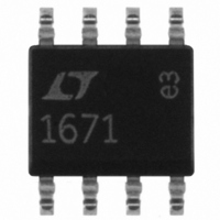
LT1671CS8#PBF Linear Technology, LT1671CS8#PBF Datasheet - Page 9

LT1671CS8#PBF
Manufacturer Part Number
LT1671CS8#PBF
Description
IC COMP GRND-SENSNG LOWPWR 8SOIC
Manufacturer
Linear Technology
Type
with Latchr
Datasheet
1.LT1671CS8PBF.pdf
(12 pages)
Specifications of LT1671CS8#PBF
Number Of Elements
1
Output Type
CMOS, Complementary, TTL
Mounting Type
Surface Mount
Package / Case
8-SOIC (0.154", 3.90mm Width)
Comparator Type
General Purpose
No. Of Comparators
1
Response Time
60ns
Ic Output Type
CMOS, MOS, Open-Collector / Drain, TTL
Supply Current
450µA
Rohs Compliant
Yes
Number Of Elements
1
Input Offset Voltage
2.5mV
Input Bias Current (typ)
280nA
Single Supply Voltage (typ)
5V
Dual Supply Voltage (typ)
±5V
Supply Current (max)
0.8@±5VmA
Power Supply Requirement
Single/Dual
Common Mode Rejection Ratio
100dB
Voltage Gain In Db
73.98dB
Power Supply Rejection Ratio
85dB
Operating Temp Range
-40C to 85C
Operating Temperature Classification
Industrial
Mounting
Surface Mount
Pin Count
8
Package Type
SOIC N
Output Compatibility
CMOS, TTL
Lead Free Status / RoHS Status
Lead free / RoHS Compliant
Available stocks
Company
Part Number
Manufacturer
Quantity
Price
APPLICATIONS
Figure 5 is a very versatile stage. It features a bipolar swing
that is set by the output transistor’s supplies. This 3ns
delay stage is ideal for driving FET switch gates. Q1, a
gated current source, switches the Baker-clamped output
transistor, Q2. The heavy feedforward capacitor from the
RISE TIME = 4ns
FALL TIME = 5ns
Figure 4. Level Shift Has Noninverting Voltage Gain
+
–
LT1671
Figure 3. Simplified LT1671 Output Stage
+V
INPUT
OUTPUT = 0
RISE TIME = 3ns
FALL TIME = 3ns
U
1k
2N2369
+
–
INFORMATION
LT1671
1000pF
U
+V (TYPICALLY 3V TO 4V)
12pF
Figure 5. Level Shift with Inverting Voltage Gain—Bipolar Swing
HP5082-2810
W
1k
1N4148
1671 F03
0.1 F
15V
2N3866
1k
5V
4.7k
820
U
1671 F04
OUT
Q1
2N2907
430
820
HP5082-2810
–10V (TYP)
5V (TYP)
LT1671 is the key to low delay, providing Q2’s base with
nearly ideal drive. This capacitor loads the LT1671’s
output transition, but Q2’s switching is clean with 3ns
delay on the rise and fall of the pulse. Figure 6 is similar to
Figure 4 except that a sink transistor has replaced the
Schottky diode. The two emitter-followers drive a power
MOSFET that switches 1A at 15V. Most of the 7ns to 9ns
delay in this stage occurs in the MOSFET and the 2N2369.
When designing level shifters, remember to use transis-
tors with fast switching times and high f
of results shown, switching times in the nanosecond
range and an f
Q2
2N2369
330
RISE TIME = 7ns
FALL TIME = 9ns
+
–
LT1671
Figure 6. Noninverting Voltage Gain Level Shift
OUTPUT
–10V
T
5V
approaching 1GHz are required.
1k
2N2369
(SHOWN IN HEAVY LINES)
CAN BE REFERENCED ANYWHERE
BETWEEN 15V AND –15V
OUTPUT TRANSISTOR SUPPLIES
12pF
15V
1k
2N3866
2N5160
1671 F05
T
. To get the kind
1k
LT1671
R
POWER
FET
L
1671 F06
9


