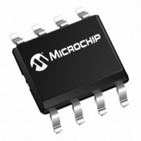
MCP6562-E/MS Microchip Technology, MCP6562-E/MS Datasheet - Page 3

MCP6562-E/MS
Manufacturer Part Number
MCP6562-E/MS
Description
IC COMP DUAL 1.8V PP 8-MSOP
Manufacturer
Microchip Technology
Type
General Purposer
Specifications of MCP6562-E/MS
Package / Case
8-TSSOP, 8-MSOP (0.118", 3.00mm Width)
Number Of Elements
2
Output Type
CMOS, Push-Pull, Rail-to-Rail, TTL
Voltage - Supply
1.8 V ~ 5.5 V
Mounting Type
Surface Mount
Mounting Style
SMD/SMT
Comparator Type
Low Power
No. Of Comparators
2
Response Time
47ns
Ic Output Type
CMOS, Push Pull, TTL
Supply Current
100µA
Supply Voltage Range
1.8V To 5.5V
Amplifier Case Style
MSOP
No. Of Pins
8
Rohs Compliant
Yes
Output Compatibility
CMOS, TTL
Lead Free Status / RoHS Status
Lead free / RoHS Compliant
Available stocks
Company
Part Number
Manufacturer
Quantity
Price
Part Number:
MCP6562-E/MS
Manufacturer:
MICROCHIP/微芯
Quantity:
20 000
1.0
1.1
V
All other inputs and outputs............V
Difference Input voltage ......................................|V
Output Short Circuit Current .................................... ±25 mA
Current at Input Pins .................................................. ±2 mA
Current at Output and Supply Pins .......................... ±50 mA
Storage temperature ................................... -65°C to +150°C
Ambient temp. with power applied .............. -40°C to +125°C
Junction temp............................................................ +150°C
ESD protection on all pins (HBM/MM)..................≥ 4 kV/300V
DC CHARACTERISTICS
© 2009 Microchip Technology Inc.
Electrical Characteristics: Unless otherwise indicated: V
R
Power Supply
Supply Voltage
Quiescent Current per comparator
Power Supply Rejection Ratio
Input
Input Offset Voltage
Input Offset Drift
Input Offset Current
Input Bias Current
Input Hysteresis Voltage
Input Hysteresis Linear Temp. Co.
Input Hysteresis Quadratic Temp.
Co.
Common-Mode Input Voltage
Range
Common-Mode Rejection Ratio
Common Mode Input Impedance
Differential Input Impedance
Push-Pull Output
High Level Output Voltage
Low Level Output Voltage
Short Circuit Current
Output Pin Capacitance
Note 1:
DD
L
= 10 kΩ to V
- V
SS
2:
3:
ELECTRICAL
CHARACTERISTICS
Maximum Ratings*
....................................................................... 6.5V
Parameters
The input offset voltage is the center of the input-referred trip points. The input hysteresis is the difference between the
input-referred trip points.
V
Limit the output current to Absolute Maximum Rating of 50 mA.
HYST
DD
/2 (see
at different temperatures is estimated using V
Figure
1-1).
SS
ΔV
Symbol
CMRR
- 0.3V to V
PSRR
V
V
Z
C
V
V
Z
V
TC
TC
V
OS
I
HYST
CMR
DIFF
I
I
OS
I
CM
OUT
DD
OS
OH
SC
Q
OL
B
/ΔT
1
2
V
V
V
DD
DD
SS
SS
DD
Min
1.8
-10
1.0
60
63
54
50
54
—
—
—
—
—
—
—
—
—
—
—
—
−0.2
−0.3
+ 0.3V
−0.7
- V
SS
DD
|
10
10
1500
Typ
100
±30
0.3
= +1.8V to +5.5V, V
±
70
60
10
66
63
65
—
±
±
—
—
—
—
—
13
13
1
8
3
2
1
||4
||2
HYST
V
V
(T
*Notice: Stresses above those listed under “Maximum Rat-
ings” may cause permanent damage to the device. This is a
stress rating only and functional operation of the device at
those or any other conditions above those indicated in the
operational listings of this specification is not implied. Expo-
sure to maximum rating conditions for extended periods may
affect device reliability.
DD
DD
5000
Max
+10
130
5.5
5.0
0.6
—
—
—
—
—
—
—
—
—
—
—
—
—
—
—
A
+0.2
+0.3
) = V
MCP6561/1R/1U/2/4
HYST @ +25°C
µV/°C
µV/°C
µV/°C
SS
Units
Ω||pF
Ω||pF
mV
mV
mA
µA
dB
pA
pA
pA
pA
dB
dB
dB
pF
V
V
V
V
V
= GND, T
2
I
V
V
V
V
T
T
T
V
V
V
V
V
V
I
(Note 3)
I
(Note 3)
Note 3
OUT
OUT
OUT
A
A
A
CM
CM
CM
CM
CM
DD
DD
CM
CM
CM
+ (T
= +25°C, V
= +85°C, V
= +125°C, V
A
= -0.3V to V
= V
= -0.3V to V
= 1.8V
= 5.5V
= V
= V
= V
= V
= V
= -3 mA/-8 mA with V
= 0
= 3 mA/8 mA with V
= +25°C, V
A
DD
- 25°C) TC
SS
SS
SS
SS
SS
/2 to V
(Note 1)
(Notes 1, 2)
IN
IN
Conditions
IN
- = V
- = V
DD
DD
IN
DD
- = V
+ = V
+0.3V, V
/2, V
1
+0.3V, V
+ (T
DD
DD
DD
/2
/2
DS22139B-page 3
DD
DD
A
/2
DD
DD
- 25°C)
/2, V
= 5.5V
DD
DD
= 1.8V/5.5V
= 1.8V/5.5V
= 5.5V
IN
= 5.5V
- = V
2
TC
SS
2
.
,


