MC10E1652FNG ON Semiconductor, MC10E1652FNG Datasheet
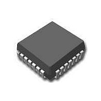
IC COMPARATOR DUAL ECL 20PLCC

MC10E1652FNG

Manufacturer Part Number
MC10E1652FNG
Description
IC COMPARATOR DUAL ECL 20PLCC
Manufacturer
ON Semiconductor
Series
MOSAIC III™r
Type
with Latchr
Datasheet

Specifications of MC10E1652FNG

Number Of Elements
2
Output Type
Differential, ECL
Mounting Type
Surface Mount
Package / Case
20-LCC (J-Lead)
Number Of Channels
2 Channels
Product
Analog Comparators
Response Time
475 ps
Supply Voltage (max)
5 V
Supply Voltage (min)
- 5.2 V
Supply Current (max)
50 mA
Maximum Operating Temperature
+ 85 C
Mounting Style
SMD/SMT
High Level Output Current
150 uA
Minimum Operating Temperature
0 C
Propagation Delay Time
925 ps
Lead Free Status / RoHS Status
Lead free / RoHS Compliant
Other names
MC10E1652FNGOS

Available stocks

Company
Part Number
Manufacturer
Quantity
Price
Part Number:
MC10E1652FNG
Manufacturer:
ON Semiconductor
Quantity:
135
Part Number:
MC10E1652FNG
Manufacturer:
ON Semiconductor
Quantity:
10 000
MC10E1652
5V, −5V ECL Dual ECL Output
Comparator with Latch
MOSAIC IIIt process and is output compatible with 10H logic
devices. In addition, the device is available in both a 16-pin DIP and a
20-pin surface mount package. However, the MC10E1652 provides
user programmable hysteresis.
ECL 10H logic levels. When the latch enable is at a logic high level,
the MC10E1652 acts as a comparator; hence, Q will be at a logic high
level if V1 > V2 (V1 is more positive than V2). Q is the complement
of Q. When the latch enable input goes to a low logic level, the outputs
are latched in their present state, providing the latch enable setup and
hold time constraints are met. The level of input hysteresis is
controlled by applying a bias voltage to the HYS pin.
Features
*For additional information on our Pb−Free strategy and soldering details, please
© Semiconductor Components Industries, LLC, 2006
November, 2006 − Rev. 9
download the ON Semiconductor Soldering and Mounting Techniques
Reference Manual, SOLDERRM/D.
The MC10E1652 is fabricated using ON Semiconductor’s advanced
The latch enable (LEN
For Additional Information, see Application Note AND8003/D
Oxygen Index: 28 to 34
Typical 3.0 dB Bandwidth > 1.0 GHz
Typical V to Q Propagation Delay of 775 ps
Typical Output Rise/Fall of 350 ps
Common Mode Range −2.0 V to +3.0 V
Individual Latch Enables
Differential Outputs
Operating Mode: V
Programmable Input Hysteresis
No Internal Input Pulldown Resistors
ESD Protection: Human Body Model; > 2 kV,
Meets or Exceeds JEDEC Spec EIA/JESD78 IC Latchup Test
Moisture Sensitivity Level 1
Flammability Rating: UL 94 V−O @ 0.125 in,
Transistor Count = 85 devices
Pb−Free Packages are Available*
Machine Model; > 100 V
CC
a
= 5.0 V, V
and LEN
b
EE
) input pins operate from standard
= −5.2 V, GND = 0 V
1
See detailed ordering and shipping information in the package
dimensions section on page 7 of this data sheet.
20 1
CASE 620A
FN SUFFIX
CASE 775
L SUFFIX
PLCC−20
CDIP−16
ORDERING INFORMATION
A
WL
YY
WW
G
http://onsemi.com
= Assembly Location
= Wafer Lot
= Year
= Work Week
= Pb−Free Package
Publication Order Number:
16
1
DIAGRAMS
MC10E1652L
AWLYYWW
MARKING
AWLYYWW
MC10E1652/D
1652FNG
MC10E
1 20

Related parts for MC10E1652FNG

MC10E1652FNG Summary of contents

Page 1

... Transistor Count = 85 devices • Pb−Free Packages are Available* *For additional information on our Pb−Free strategy and soldering details, please download the ON Semiconductor Soldering and Mounting Techniques Reference Manual, SOLDERRM/D. © Semiconductor Components Industries, LLC, 2006 November, 2006 − Rev −5.2 V, GND = 0 V See detailed ordering and shipping information in the package dimensions section on page 7 of this data sheet ...

Page 2

Qb LEN GND Pinout: 20-Lead PLCC (Top View) GND LEN All V Warning: All V connected to Power Supply to ...

Page 3

Table 3. MAXIMUM RATINGS Symbol Parameter VSUP Total Supply Voltage VPP Differential Input Voltage V Input Voltage I I Output Current out I V Sink/Source Operating Temperature Range T Storage Temperature Range stg q Thermal Resistance (Junction ...

Page 4

HYSTERESIS −1.2 −1.4 −1.6 −1.8 −20 −16 −12 −8 −4 Vref Vin, DIFFERENTIAL INPUT VOLTAGE (mV) Figure 3. Typical Hysteresis Curve Table 5. AC CHARACTERISTICS V Symbol Characteristic f Maximum Toggle Frequency MAX t Propagation Delay to Output ...

Page 5

The timing diagram (Figure 5.) is presented to illustrate the MC10E1652’s compare and latch features. When the signal on the LEN pin logic high level, the device is operating in the “compare mode,” and the signal on ...

Page 6

Under a constant set of input conditions comparators have a specified nominal propagation delay. However, since propagation delay is a function of input slew rate and input voltage overdrive the delay dispersion parameters are provided to allow ...

Page 7

... Application Note AND8020 − Termination of ECL Logic Devices.) ORDERING INFORMATION Device MC10E1652L MC10E1652FN MC10E1652FNG MC10E1652FNR2 MC10E1652FNR2G †For information on tape and reel specifications, including part orientation and tape sizes, please refer to our Tape and Reel Packaging Specifications Brochure, BRD8011/D. Resource Reference of Application Notes ...

Page 8

0.25 (0.010) PACKAGE DIMENSIONS CDIP−16 L SUFFIX CERAMIC DIP PACKAGE CASE 620A−01 ISSUE 16X 0.25 (0.010 SEATING T PLANE ...

Page 9

Y BRK −L− −M− 0.007 (0.180) Z 0.007 (0.180 −T− J VIEW S G1 0.010 (0.250) T L− NOTES: 1. DIMENSIONS AND TOLERANCING PER ANSI Y14.5M, ...

Page 10

... Opportunity/Affirmative Action Employer. This literature is subject to all applicable copyright laws and is not for resale in any manner. PUBLICATION ORDERING INFORMATION LITERATURE FULFILLMENT: Literature Distribution Center for ON Semiconductor P.O. Box 5163, Denver, Colorado 80217 USA Phone: 303−675−2175 or 800−344−3860 Toll Free USA/Canada Fax: 303− ...

Related keywords