LMH0303SQE/NOPB National Semiconductor, LMH0303SQE/NOPB Datasheet - Page 6
LMH0303SQE/NOPB
Manufacturer Part Number
LMH0303SQE/NOPB
Description
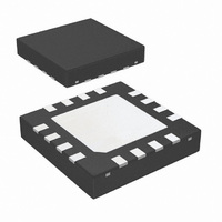
IC CABLE DVR 3G HD/SD SDI 16LLP
Manufacturer
National Semiconductor
Type
Driverr
Datasheet
1.LMH0303SQENOPB.pdf
(14 pages)
Specifications of LMH0303SQE/NOPB
Applications
Amplifiers, Video Distribution
Package / Case
16-LLP
Leaded Process Compatible
Yes
Rohs Compliant
Yes
Peak Reflow Compatible (260 C)
Yes
Operating Temperature (min)
-40C
Operating Temperature Classification
Industrial
Operating Temperature (max)
85C
Package Type
LLP EP
Rad Hardened
No
Lead Free Status / RoHS Status
Lead free / RoHS Compliant
Mounting Type
-
Lead Free Status / Rohs Status
Compliant
Other names
LMH0303SQETR


www.national.com
Timing Diagram
Device Operation
INPUT INTERFACING
The LMH0303 accepts either differential or single-ended in-
put. For single-ended operation, the unused input must be
properly terminated.
OUTPUT INTERFACING
The LMH0303 uses current mode outputs. Single-ended out-
put levels are 800 mV
with an R
between the R
should be used for R
The R
the R
the R
capacitance.
OUTPUT SLEW RATE CONTROL
The LMH0303 output rise and fall times are selectable for ei-
ther SMPTE 259M or SMPTE 424M / 292M compliance via
the SD/HD pin. For slower rise and fall times, or SMPTE 259M
compliance, SD/HD is set high. For faster rise and fall times,
or SMPTE 424M and SMPTE 292M compliance, SD/HD is
set low. SD/HD may also be controlled using the SMBus, pro-
vided the SD/HD pin is held low. SD/HD has an internal
pulldown.
OUTPUT ENABLE
The SDO/SDO output driver can be enabled or disabled with
the ENABLE pin. When set low, the output driver is powered
off and the LMH0303 enters a deep power save mode. EN-
ABLE has an internal pullup.
INPUT LOS OF SIGNAL DETECTION (LOS)
The LMH0303 detects when the input signal does not have a
video-like pattern. Self oscillation and low levels of noise are
rejected. This loss of signal detect allows a very sensitive in-
put stage that is robust against coupled noise without any
degradation of jitter performance.
Via the SMBus, the loss of signal detect can either add an
input offset or mute the outputs. An offset is added by default.
Additionally, the loss of signal detect can be linked to the EN-
ABLE functionality so that when the LOS goes low, ENABLE
will also go low.
OUTPUT CABLE DETECTION
The LMH0303 detects when an output is locally terminated.
When a video signal (or AC test signal) is present on SDI, the
device senses the SDO and SDO amplitudes. If the output is
not properly terminated (via a terminated cable or local ter-
REF
REF
REF
pin. In addition, the copper in the plane layers below
REF
network should be removed to minimize parasitic
resistor should be placed as close as possible to
resistor of 750Ω. The R
REF
pin and V
REF
P-P
is 750Ω.
into 75Ω AC-coupled coaxial cable
CC
. The only resistor value that
REF
resistor is connected
SMBus Timing Parameters
6
mination), the amplitude will be higher than expected, and the
Termination Fault signal is asserted. The Termination Fault
signal is de-asserted when the proper termination is applied.
This feature allows the system designer the flexibility to react
to cable attachment and removal. Note that a long length of
cable will look like a proper termination at the device output.
The cable driver must be enabled for the termination detection
to operate. If the Termination Fault will be used to power down
the LMH0303, then periodic polling (enabling) is recommend-
ed to monitor the output termination. For example, when a
Fault condition is triggered, ENABLE can be driven low to
power down the device. The LMH0303 should be re-enabled
periodically to check the status of the output termination. The
LMH0303 needs to be powered on for roughly 4 ms for Ter-
mination Fault detection to work.
SMBus Interface
The System Management Bus (SMBus) is a two-wire inter-
face designed for the communication between various sys-
tem component chips. By accessing the control functions of
the circuit via the SMBus, pincount is kept to a minimum while
allowing a maximum amount of versatility. The LMH0303 has
several internal configuration registers which may be ac-
cessed via the SMBus.
The 7-bit default address for the LMH0303 is 17h. The LSB
is set to 0b for a WRITE and 1b for a READ, so the 8-bit default
address for a WRITE is 2Eh and the 8-bit default address for
a READ is 2Fh. The SMBus address may be dynamically
changed.
In applications where there might be several LMH0303s, the
SDA, SCL, and FAULT pins can be shared. The SCL, SDA,
and FAULT pins are open drain and require external pullup
resistors. Multiple LMH0303s may have the FAULT pin wire
ORed. This signal becomes active when either loss of signal
is detected or any termination faults are detected. The regis-
ters may be read in order to determine the cause. Additionally,
each signal can be masked from the FAULT pin.
TRANSFER OF DATA VIA THE SMBus
During normal operation the data on SDA must be stable dur-
ing the time when SCL is High.
There are three unique states for the SMBus:
START: A High-to-Low transition on SDA while SCL is High
indicates a message START condition.
STOP: A Low-to-High transition on SDA while SCL is High
indicates a message STOP condition.
IDLE: If SCL and SDA are both High for a time exceeding
t
for a total exceeding the maximum specification for t
the bus will transfer to the IDLE state.
BUF
from the last detected STOP condition or if they are High
HIGH
then
30043206
Related parts for LMH0303SQE/NOPB
Image
Part Number
Description
Manufacturer
Datasheet
Request
R

Part Number:
Description:
IC CABLE DVR 3G HD/SD SDI 16LLP
Manufacturer:
National Semiconductor
Datasheet:

Part Number:
Description:
3 Gbps Hd/sd Sdi Cable Driver With Cable Detect
Manufacturer:
National Semiconductor Corporation

Part Number:
Description:
National Semiconductor [8-Bit D/A Converter]
Manufacturer:
National Semiconductor
Datasheet:
Part Number:
Description:
National Semiconductor [Media Coprocessor]
Manufacturer:
National Semiconductor
Datasheet:
Part Number:
Description:
Digitally Controlled Tone and Volume Circuit with Stereo Audio Power Amplifier, Microphone Preamp Stage and National 3D Sound
Manufacturer:
National Semiconductor
Datasheet:
Part Number:
Description:
Digitally Controlled Tone and Volume Circuit with Stereo Audio Power Amplifier, Microphone Preamp Stage and National 3D Sound
Manufacturer:
National Semiconductor
Datasheet:
Part Number:
Description:
AC97 Rev 2 Codec with Sample Rate Conversion and National 3D Sound
Manufacturer:
National Semiconductor
Part Number:
Description:
Manufacturer:
National Semiconductor
Datasheet:
Part Number:
Description:
Manufacturer:
National Semiconductor
Datasheet:
Part Number:
Description:
General Purpose, Low Voltage, Low Power, Rail-to-Rail Output Operational Amplifiers
Manufacturer:
National Semiconductor
Datasheet:
Part Number:
Description:
8-bit 20 MSPS flash A/D converter.
Manufacturer:
National Semiconductor
Datasheet:
Part Number:
Description:
Low Noise Quad Operational Amplifier
Manufacturer:
National Semiconductor
Datasheet:
Part Number:
Description:
Quad Differential Line Receivers
Manufacturer:
National Semiconductor
Datasheet:
Part Number:
Description:
Quad High Speed Trapezoidal? Bus Transceiver
Manufacturer:
National Semiconductor
Datasheet: