PI74AVC164245LAAE Pericom Semiconductor, PI74AVC164245LAAE Datasheet - Page 2
PI74AVC164245LAAE
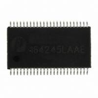
Manufacturer Part Number
PI74AVC164245LAAE
Description
IC TXRX LEVEL SHIFT 3ST 48-TSSOP
Manufacturer
Pericom Semiconductor
Series
74AVCr
Datasheet
1.PI74AVC164245LAAE.pdf
(10 pages)
Specifications of PI74AVC164245LAAE
Logic Function
Level Shifter, 3-State
Number Of Bits
16
Input Type
Voltage
Output Type
Voltage
Number Of Channels
2
Number Of Outputs/channel
8
Differential - Input:output
No/No
Propagation Delay (max)
4.2ns
Voltage - Supply
2.3 V ~ 2.7 V, 3 V ~ 3.6 V
Operating Temperature
-40°C ~ 85°C
Package / Case
48-TSSOP
Mounting Type
Surface Mount
Logic Type
Transceiver, Non-Inverting
Current - Output High, Low
12mA, 12mA
Number Of Elements
2
Number Of Bits Per Element
8
Logic Family
PI74AVC164245LA
Number Of Channels Per Chip
16
Input Level
CMOS
Output Level
CMOS
High Level Output Current
- 12 mA
Low Level Output Current
12 mA
Propagation Delay Time
3.5 ns
Supply Voltage (max)
2.7 V, 3.6 V
Supply Voltage (min)
1.4 V, 3 V
Maximum Operating Temperature
+ 85 C
Function
Bus Transceiver with Voltage Translation
Input Bias Current (max)
30 uA
Minimum Operating Temperature
- 40 C
Mounting Style
SMD/SMT
Number Of Circuits
2
Polarity
Non-Inverting
Lead Free Status / RoHS Status
Lead free / RoHS Compliant
Available stocks
Company
Part Number
Manufacturer
Quantity
Price


1 2 3 4 5 6 7 8 9 0 1 2 3 4 5 6 7 8 9 0 1 2 3 4 5 6 7 8 9 0 1 2 1 2 3 4 5 6 7 8 9 0 1 2 3 4 5 6 7 8 9 0 1 2 3 4 5 6 7 8 9 0 1 2 1 2 3 4 5 6 7 8 9 0 1 2 3 4 5 6 7 8 9 0 1 2 3 4 5 6 7 8 9 0 1 2 1 2 3 4 5 6 7 8 9 0 1 2 3 4 5 6 7 8 9 0 1 2 3 4 5 6 7 8 9 0 1 2 1 2 3 4 5 6 7 8 9 0 1 2
1 2 3 4 5 6 7 8 9 0 1 2 3 4 5 6 7 8 9 0 1 2 3 4 5 6 7 8 9 0 1 2 1 2 3 4 5 6 7 8 9 0 1 2 3 4 5 6 7 8 9 0 1 2 3 4 5 6 7 8 9 0 1 2 1 2 3 4 5 6 7 8 9 0 1 2 3 4 5 6 7 8 9 0 1 2 3 4 5 6 7 8 9 0 1 2 1 2 3 4 5 6 7 8 9 0 1 2 3 4 5 6 7 8 9 0 1 2 3 4 5 6 7 8 9 0 1 2 1 2 3 4 5 6 7 8 9 0 1 2
Maximum Ratings
(Absolute maximum ratings over operating free-air temperature range from V
Note:
Stresses greater than those listed under MAXIMUM RATINGS may cause permanent damage to the device. This is a stress rating only and
functional operation of the device at these or any other conditions above those indicated in the operational sections of this specification is not
implied. Exposure to absolute maximum rating conditions for extended periods may affect reliability.
Recommended Operating Conditions for V
Recommended Operating Conditions for V
Notes:
1. This value is limited to 4.6V maximum.
2. This value is limited to 3.8V maximum.
3. The package thermal impedance is calculated in accordance with JESD 51.
4. To ensure proper device operation, all unused device inputs must be held at the associated V
Supply voltage range:
Input Voltage Range, V
Input clamp current, I
Output clamp current, I
V
V
08-0291
V
V
C
V
C
V
V
I
V
V
V
I
I
I
T
T
/ t v
/ t v
O
O
O
O
C
O
C
O
H I
H I
A I
L I
B I
A
L I
A
H
H
L
L
A
A
B
B
(
(
) 2
) 1
IK
S
O
O
i H
L
I
i H
L
I
OK
p n
p n
I
S
O
O
i H
L
I
i H
L
I
u
(V
o
o
u
p
p n
p n
h g
h g
p p
u
o
o
w
w
V
V
Except I/O ports
I/O port A
I/O port B
p t
u
p
r e
t u
t u
h g
h g
p p
(V
w
w
I
p t
r e
t u
t u
l -
l -
e l -
e l -
CCA ..................................
CCB ..................................
t u
y l
i t a
<0) .................................... –50mA
l -
l -
e l -
e l -
o v
a r t
t u
v e
v e
y l
i t a
O
V
a r t
e v
e v
v e
v e
g n
o v
o v
l e
l e
a t l
e v
e v
s n
<0) .............................. –50mA
o
g n
o v
V
o l
o l
l e
l e
s n
a t l
a t l
a t l
o
e r f
e g
i t i
o v
o v
o l
o l
a t l
a t l
e r f
i t i
o v
o v
t u
t u
e g
e g
e g
n o
- e
a t l
a t l
t u
t u
e g
n o
(1)
e g
u p
u p
(2)
- e
a t l
a t l
u p
u p
r i a
r
e g
e g
e s i
c t
c t
r i a
e g
e g
r
... –0.5V to V
.... –0.5V to V
c t
c t
e s i
e t
r u
r u
e t
o
r u
r u
m
(1)
e r
e r
o
f r
m
e p
e r
e r
f r
t n
t n
......–0.5V to 4.6V
e p
l l a
t n
t n
a r
l l a
a r
a r
u t
–0.5V to 3.8V
–0.5V to 4.6V
a r
u t
e t
e r
e t
e r
CCA
CCB
CCA
CCB
+0.5V
+0.5V
at 3.3V
at 2.5V
V
V
V
V
V
V
C
C
C
C
C
C
C
C
C
C
C
C
2
A
A
A
A
A
A
(4)
(4)
=
=
=
=
=
=
Continuous output current, I
Continuous current through each V
Package thermal impedance, 0
Storage temperature range, T
2
2
2
2
2
2
3 .
3 .
3 .
7 .
3 .
7 .
V
V
V
V
V
V
CCB
o t
o t
2
2
at 3.3V & V
M
7 .
7 .
–
3
0 4
2
0
0
V
V
0 .
. n i
16-Bit 1.5-2.5V to 3.3V Level Shifting
CC
CCA
or GND.
Transceiver with 3-State Outputs
K package ............................ 58°C/W
V package ............................ 94°C/W
at 1.5 - 2.5V, unless otherwise noted)
M
–
2
1
O ...............................................
STG ...........................
0
0
0 4
3 .
7 .
. n i
JA
M
V
V
(3)
–
3
0
0 1
5 8
C
C
2 1
2 1
a
6 .
8 .
C
C
: A package .......... 89°C/W
CC
. x
B
B
or GND ...........±100mA
PI74AVC164245LA
M
V
V
–
2
0
8 –
C
C
5 8
2 1
0 1
2 1
8
a
7 .
7 .
C
C
. x
A
A
–65°C to 150°C
PS8600C
U
s n
m
C °
n
V
V /
U
A
s t i
s n
m
±50mA
C °
n
V
V /
A
s t i
11/06/08
Related parts for PI74AVC164245LAAE
Image
Part Number
Description
Manufacturer
Datasheet
Request
R

Part Number:
Description:
48/16 BIT EDGE TRIGGERED DTYPE
Manufacturer:
Pericom Semiconductor
Part Number:
Description:
56/2.5V, 20-BIT UNIVERSAL BUS
Manufacturer:
Pericom Semiconductor
Part Number:
Description:
IC BUFF DVR TRI-ST 16BIT 48TSSOP
Manufacturer:
Pericom Semiconductor
Datasheet:
Part Number:
Description:
IC TXRX BIDIR 16BIT 3ST 48-TSSOP
Manufacturer:
Pericom Semiconductor
Datasheet:
Part Number:
Description:
IC UNIV BUS DVR 20BIT 56TSSOP
Manufacturer:
Pericom Semiconductor
Datasheet:
Part Number:
Description:
IC BUFF DVR TRI-ST 16BIT 48TVSOP
Manufacturer:
Pericom Semiconductor
Datasheet:
Part Number:
Description:
IC TXRX BIDIR 16BIT 3ST 48-TVSOP
Manufacturer:
Pericom Semiconductor
Datasheet:
Part Number:
Description:
IC ADRSS DRVR REG 1-4BIT 56TSSOP
Manufacturer:
Pericom Semiconductor
Datasheet:
Part Number:
Description:
IC BUS TXRX/REG 16BT 3ST 56TSSOP
Manufacturer:
Pericom Semiconductor
Datasheet:
Part Number:
Description:
IC BUFF DVR TRI-ST 16BIT 48TSSOP
Manufacturer:
Pericom Semiconductor
Datasheet:
Part Number:
Description:
IC FLIP FLOP 3ST 10BIT 56TSSOP
Manufacturer:
Pericom Semiconductor
Part Number:
Description:
IC FLIP FLOP 3ST 10BIT 56TSSOP
Manufacturer:
Pericom Semiconductor
Datasheet:
Part Number:
Description:
IC FLIP FLOP 3ST 10BIT 56TSSOP
Manufacturer:
Pericom Semiconductor
Datasheet:
Part Number:
Description:
IC D-TYP F/F 16BIT 3-ST 48-TSSOP
Manufacturer:
Pericom Semiconductor
Datasheet:
Part Number:
Description:
IC F/F 20BIT TRI-ST 56-TSSOP
Manufacturer:
Pericom Semiconductor
Datasheet: