IDT74LVCH16543APAG IDT, Integrated Device Technology Inc, IDT74LVCH16543APAG Datasheet - Page 2
IDT74LVCH16543APAG
Manufacturer Part Number
IDT74LVCH16543APAG
Description
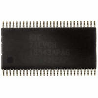
IC TRSCVR TRI-ST 16BIT 56TSSOP
Manufacturer
IDT, Integrated Device Technology Inc
Series
74LVCHr
Datasheet
1.IDT74LVCH16543APAG.pdf
(6 pages)
Specifications of IDT74LVCH16543APAG
Logic Type
Transceiver, Non-Inverting
Number Of Elements
2
Number Of Bits Per Element
8
Current - Output High, Low
24mA, 24mA
Voltage - Supply
2.7 V ~ 3.6 V
Operating Temperature
-40°C ~ 85°C
Mounting Type
Surface Mount
Package / Case
56-TSSOP
Lead Free Status / RoHS Status
Lead free / RoHS Compliant
Other names
74LVCH16543APAG
800-1689
800-1689-5
800-1689
800-1689
800-1689-5
800-1689


NOTE:
1. As applicable to the device type.
PIN CONFIGURATION
CAPACITANCE
IDT74LVCH16543A
3.3V CMOS 16-BIT REGISTERED TRANSCEIVER WITH 3-STATE OUTPUTS
C
Symbol
C
C
IN
OUT
I/O
Input Capacitance
Output Capacitance
I/O Port Capacitance
2
1
2
1
1
2
CEAB
OEAB
OEAB
CEAB
LEAB
LEAB
Parameter
GND
GND
GND
GND
V
V
1
1
1
1
1
1
2
2
2
2
2
2
1
2
1
2
A
A
A
A
A
A
A
A
A
A
A
A
A
A
CC
CC
A
A
2
3
4
5
6
7
8
2
3
4
5
6
7
8
1
1
(1)
1
10
11
12
13
14
15
16
17
18
19
2
3
4
5
6
7
8
9
20
21
22
23
24
25
26
27
28
(T
TOP VIEW
A
TSSOP
= +25°C, F = 1.0MHz)
Conditions
V
V
V
OUT
IN
IN
= 0V
= 0V
= 0V
45
56
55
54
53
52
51
50
48
47
46
44
43
42
41
40
38
37
36
35
34
33
32
31
30
29
49
39
Typ.
4.5
6.5
6.5
1
1
1
1
1
1
1
1
1
1
1
2
GND
V
GND
2
2
2
GND
2
2
2
V
2
2
GND
2
2
OEBA
LEBA
CEBA
B
B
B
B
B
B
B
B
CEBA
B
B
B
B
B
B
B
B
LEBA
OEBA
CC
CC
1
2
3
4
5
6
7
8
1
2
3
4
5
6
7
8
Max.
6
8
8
Unit
pF
pF
pF
2
NOTE:
1. Stresses greater than those listed under ABSOLUTE MAXIMUM RATINGS may cause
PIN DESCRIPTION
NOTE:
1. These pins have "Bus-Hold". All other pins are standard inputs, outputs, or I/Os.
FUNCTION TABLE
ABSOLUTE MAXIMUM RATINGS
NOTES:
1. H = HIGH Voltage Level
2. A-to-B data flow is shown. B-to-A data flow is similar but uses xCEBA, xLEBA, and
3. Before xLEAB LOW-to-HIGH transition.
Symbol
V
T
I
I
I
I
I
xCEAB
CC
OUT
IK
OK
SS
Pin Names
STG
TERM
permanent damage to the device. This is a stress rating only and functional operation
of the device at these or any other conditions above those indicated in the operational
sections of this specification is not implied. Exposure to absolute maximum rating
conditions for extended periods may affect reliability.
L = LOW Voltage Level
X = Don’t Care
Z = High-Impedance
xOEBA.
xOEAB
xOEBA
xCEAB
xCEBA
xLEAB
xLEBA
H
X
L
L
L
L
X
x A x
x B x
Terminal Voltage with Respect to GND
Storage Temperature
DC Output Current
Continuous Clamp Current,
V
Continuous Current through each
V
xLEAB
I
CC
Inputs
< 0 or V
H
H
H
X
X
L
L
or GND
O
A-to-B Output Enable Input (Active LOW)
B-to-A Output Enable Input (Active LOW)
A-to-B Enable Input (Active LOW)
B-to-A Enable Input (Active LOW)
A-to-B Latch Enable Input (Active LOW)
B-to-A Latch Enable Input (Active LOW)
A-to-B Data Inputs or B-to-A 3-State Outputs
B-to-A Data Inputs or A-to-B 3-State Outputs
Description
< 0
xOEAB
H
H
H
X
L
L
X
INDUSTRIAL TEMPERATURE RANGE
(EACH 8-BIT SECTION)
Description
Latch Status
xAx to xBx
Transparent
Transparent
Storing
Storing
Storing
Storing
Storing
–0.5 to +6.5
–65 to +150
–50 to +50
±100
Previous
Max
Not Recommended
–50
Current A Inputs
Output Buffers
High Z
High Z
High Z
High Z
(1,2)
(1)
(1)
(1)
xBx
(3)
A Inputs
Unit
mA
mA
mA
° C
V
Related parts for IDT74LVCH16543APAG
Image
Part Number
Description
Manufacturer
Datasheet
Request
R

Part Number:
Description:
TRANSLATION DEVICE DPI 80-PQFP
Manufacturer:
IDT, Integrated Device Technology Inc
Datasheet:
Part Number:
Description:
IDT PART
Manufacturer:
IDT, Integrated Device Technology Inc
Datasheet:
Part Number:
Description:
IC LIU T1/E1/J1 OCTAL 256PBGA
Manufacturer:
IDT, Integrated Device Technology Inc
Datasheet:

Part Number:
Description:
IC FREQ TIMING GENERATOR 28TSSOP
Manufacturer:
IDT, Integrated Device Technology Inc
Datasheet:
Part Number:
Description:
IC CLK DVR PLL 1:10 40VFQFPN
Manufacturer:
IDT, Integrated Device Technology Inc
Datasheet:
Part Number:
Description:
IC CLK FANOUT BUFFER 1:18 32LQFP
Manufacturer:
IDT, Integrated Device Technology Inc
Datasheet:
Part Number:
Description:
IC CLK FANOUT BUFFER 1:18 32LQFP
Manufacturer:
IDT, Integrated Device Technology Inc
Datasheet:
Part Number:
Description:
IC CK505 VREG/RES 56TSSOP
Manufacturer:
IDT, Integrated Device Technology Inc
Datasheet:

Part Number:
Description:
IC SDRAM CLK DVR 1:10 48-TSSOP
Manufacturer:
IDT, Integrated Device Technology Inc
Datasheet:

Part Number:
Description:
IC CLK DVR PLL 1:10 48TSSOP
Manufacturer:
IDT, Integrated Device Technology Inc
Datasheet:
Part Number:
Description:
IC FLEXPC CLK PROGR P4 56-TSSOP
Manufacturer:
IDT, Integrated Device Technology Inc
Datasheet:
Part Number:
Description:
IC FLEXPC CLK PROGR P4 56-TSSOP
Manufacturer:
IDT, Integrated Device Technology Inc
Datasheet:
Part Number:
Description:
IC FLEXPC CLK PROGR P4 56-SSOP
Manufacturer:
IDT, Integrated Device Technology Inc
Datasheet:

Part Number:
Description:
IC PLL CLK DRIVER 2.5V 28-TSSOP
Manufacturer:
IDT, Integrated Device Technology Inc
Datasheet:
Part Number:
Description:
IC CLOCK DRIVER 2.5V 24-TSSOP
Manufacturer:
IDT, Integrated Device Technology Inc
Datasheet: