74LCXZ16244MTDX Fairchild Semiconductor, 74LCXZ16244MTDX Datasheet

IC BUFF/DVR 16BIT LOW V 48TSSOP

74LCXZ16244MTDX

Manufacturer Part Number
74LCXZ16244MTDX
Description
IC BUFF/DVR 16BIT LOW V 48TSSOP
Manufacturer
Fairchild Semiconductor
Series
74LCXZr
Datasheet

Specifications of 74LCXZ16244MTDX

Logic Type
Buffer/Line Driver, Non-Inverting
Number Of Elements
4
Number Of Bits Per Element
4
Current - Output High, Low
12mA, 12mA
Voltage - Supply
2.7 V ~ 3.6 V
Operating Temperature
-40°C ~ 85°C
Mounting Type
Surface Mount
Package / Case
48-TSSOP
Lead Free Status / RoHS Status
Lead free / RoHS Compliant
© 2005 Fairchild Semiconductor Corporation
74LCXZ162244MEA
74LCXZ162244MEX
(Note 1)
74LCXZ162244MTD
74LCXZ162244MTX
(Note 1)
74LCXZ162244
Low Voltage 16-Bit Buffer/Line Driver with 5V Tolerant
Inputs/Outputs and 26: Series Resistors in the Outputs
General Description
The LCXZ162244 contains sixteen non-inverting buffers
with 3-STATE outputs designed to be employed as a mem-
ory and address driver, clock driver, or bus oriented trans-
mitter/receiver. The device is nibble controlled. Each nibble
has separate 3-STATE control inputs which can be shorted
together for full 16-bit operation.
When V
the high impedance state during power up or power down.
this places the outputs in the high impedance (Z) state pre-
venting intermittent low impedance loading or glitching in
bus oriented applications.
The LCXZ162244 is designed for low voltage (2.7V or
3.3V) V
signal environment.
In addition the outputs include 26
tors to reduce overshoot and undershoot and are designed
to sink/source 12 mA at V
The LCXZ162244 is fabricated with an advanced CMOS
technology to achieve high speed operation while maintain-
ing CMOS low power dissipation.
Ordering Code:
Note 1: Use this Order Number to receive devices in Tape and Reel.
Order Number
CC
CC
applications with capability of interfacing to a 5V
is between 0 and 1.5V, the LCXZ162244 is in
Package
CC
Number
MS48A
MS48A
MTD48
MTD48
3.0V.
:
(nominal) series resis-
48-Lead Small Shrink Outline Package (SSOP), JEDEC MO-118, 0.300" Wide
[TUBES]
48-Lead Small Shrink Outline Package (SSOP), JEDEC MO-118, 0.300" Wide
[TAPE and REEL]
48-Lead Thin Shrink Small Outline Package (TSSOP), JEDEC MO-153, 6.1mm Wide
[TUBES]
48-Lead Thin Shrink Small Outline Package (TSSOP), JEDEC MO-153, 6.1mm Wide
[TAPE and REEL]
DS500251
Features
5V tolerant inputs and outputs
Guaranteed power up/down high impedance
Supports live insertion/withdrawal
Outputs have equivalent 26
2.7V–3.6V V
5.3 ns t
r
Implements patented noise/EMI reduction circuitry
Latch-up performance exceeds 500 mA
ESD performance:
12 mA output drive (V
Human body model
Machine model
Package Description
PD
max (V
CC
specifications provided
CC
!
200V
!
3.0V), 20
CC
2000V
:
3.0V)
September 2000
Revised June 2005
series resistors
P
A I
CC
www.fairchildsemi.com
max

Related parts for 74LCXZ16244MTDX

74LCXZ16244MTDX Summary of contents

Page 1

... Thin Shrink Small Outline Package (TSSOP), JEDEC MO-153, 6.1mm Wide (Note 1) [TAPE and REEL] Note 1: Use this Order Number to receive devices in Tape and Reel. © 2005 Fairchild Semiconductor Corporation Features 5V tolerant inputs and outputs Guaranteed power up/down high impedance Supports live insertion/withdrawal Outputs have equivalent 26 2.7V– ...

Page 2

Connection Diagram Truth Tables Inputs OE I – Inputs OE I – HIGH Voltage Level L LOW Voltage Level X Immaterial ...

Page 3

Absolute Maximum Ratings Symbol Parameter V Supply Voltage Input Voltage Output Voltage Input Diode Current Output Diode Current Output Source/Sink Current Supply ...

Page 4

DC Electrical Characteristics Note 5: Outputs disabled or 3-STATE only. AC Electrical Characteristics Symbol Parameter t Propagation Delay PHL t Data to Output PLH t Output Enable Time PZL t PZH t Output Disable Time PLZ t PHZ t Output ...

Page 5

AC LOADING and WAVEFORMS FIGURE 1. AC Test Circuit (C 6V for Waveform for Inverting and Non-Inverting Functions Propagation Delay. Pulse Width and t rec 3-STATE Output Low Enable and Disable Times for Logic (Input Characteristics; f ...

Page 6

Schematic Diagram Generic for LCX Family www.fairchildsemi.com 6 ...

Page 7

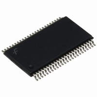
Physical Dimensions inches (millimeters) unless otherwise noted 48-Lead Small Shrink Outline Package (SSOP), JEDEC MO-118, 0.300" Wide Package Number MS48A 7 www.fairchildsemi.com ...

Page 8

Physical Dimensions inches (millimeters) unless otherwise noted (Continued) 48-Lead Thin Shrink Small Outline Package (TSSOP), JEDEC MO-153, 6.1mm Wide Fairchild does not assume any responsibility for use of any circuitry described, no circuit patent licenses are implied and Fairchild reserves ...

Related keywords