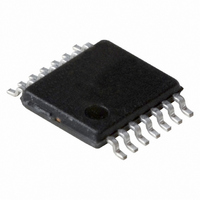
74LVC07APW,118 NXP Semiconductors, 74LVC07APW,118 Datasheet - Page 3

74LVC07APW,118
Manufacturer Part Number
74LVC07APW,118
Description
IC BUFF HEX OPEN DRAIN 14TSSOP
Manufacturer
NXP Semiconductors
Series
74LVCr
Datasheet
1.74LVC07ABQ115.pdf
(14 pages)
Specifications of 74LVC07APW,118
Logic Type
Buffer/Line Driver, Non-Inverting with Open Drain
Package / Case
14-TSSOP
Number Of Elements
6
Number Of Bits Per Element
1
Current - Output High, Low
32mA, 32mA
Voltage - Supply
2 V ~ 5.5 V
Operating Temperature
-40°C ~ 125°C
Mounting Type
Surface Mount
Logic Family
74LVC
Number Of Channels Per Chip
6
Polarity
Non-Inverting
Supply Voltage (max)
5.5 V
Supply Voltage (min)
1.65 V
Maximum Operating Temperature
125 C
Mounting Style
SMD/SMT
Input Bias Current (max)
10 uA
Low Level Output Current
32 mA
Maximum Power Dissipation
500 mW
Minimum Operating Temperature
- 40 C
Number Of Lines (input / Output)
6 / 6
Output Type
Open Drain
Propagation Delay Time
2.5 ns
Logical Function
Buffer/Driver
Number Of Elements
6
Number Of Channels
6
Number Of Inputs
6
Number Of Outputs
6
Operating Supply Voltage (typ)
1.8/2.5/3.3/5V
Package Type
TSSOP
High Level Output Current
32mA
Operating Supply Voltage (max)
5.5V
Operating Supply Voltage (min)
1.65V
Quiescent Current
10uA
Technology
CMOS
Pin Count
14
Mounting
Surface Mount
Operating Temp Range
-40C to 125C
Operating Temperature Classification
Automotive
Lead Free Status / RoHS Status
Lead free / RoHS Compliant
Lead Free Status / RoHS Status
Lead free / RoHS Compliant, Lead free / RoHS Compliant
Other names
568-2286-2
74LVC07APW-T
935265482118
74LVC07APW-T
935265482118
Philips Semiconductors
ORDERING INFORMATION
PINNING
2003 Nov 11
handbook, halfpage
74LVC07AD
74LVC07APW
74LVC07ABQ
Hex buffer with open-drain outputs
Fig.1 Pin configuration SO14 and TSSOP14.
TYPE NUMBER
PIN
10
11
12
13
14
1
2
3
4
5
6
7
8
9
GND
1A
1Y
2A
2Y
3A
3Y
1
2
3
4
5
6
7
07
MNA531
1A
1Y
2A
2Y
3A
3Y
GND
4Y
4A
5Y
5A
6Y
6A
V
TEMPERATURE RANGE
CC
14
13
12
11
10
9
8
40 to +125 C
40 to +125 C
40 to +125 C
V CC
6A
6Y
5A
5Y
4A
4Y
SYMBOL
3
data input
data output
data input
data output
data input
data output
ground (0 V)
data output
data input
data output
data input
data output
data input
supply voltage
handbook, halfpage
PINS
(1) The die substrate is attached to this pad using conductive die
14
14
14
attach material. It can not be used as a supply pin or input.
PACKAGE
Fig.2 Pin configuration DHVQFN14.
1Y
2A
2Y
3A
3Y
DHVQFN14
PACKAGE
Top view
TSSOP14
2
3
4
5
6
SO14
DESCRIPTION
GND
1A
7
1
GND
V CC
MATERIAL
(1)
4Y
14
8
plastic
plastic
plastic
Product specification
MBL760
74LVC07A
13
12
11
10
9
6A
6Y
5A
5Y
4A
SOT108-1
SOT402-1
SOT762-1
CODE


