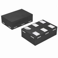
74AUP1G125GM,115 NXP Semiconductors, 74AUP1G125GM,115 Datasheet - Page 12

74AUP1G125GM,115
Manufacturer Part Number
74AUP1G125GM,115
Description
IC BUFF DVR TRI-ST LOW PWR 6XSON
Manufacturer
NXP Semiconductors
Series
74AUPr
Datasheet
1.74AUP1G125GW125.pdf
(24 pages)
Specifications of 74AUP1G125GM,115
Logic Type
Buffer/Line Driver, Non-Inverting
Number Of Elements
1
Number Of Bits Per Element
1
Current - Output High, Low
4mA, 4mA
Voltage - Supply
0.8 V ~ 3.6 V
Operating Temperature
-40°C ~ 125°C
Mounting Type
Surface Mount
Package / Case
6-XSON (Micropak™), SOT-886
Logic Family
AUP
Number Of Channels Per Chip
1
Polarity
Non-Inverting
Supply Voltage (max)
3.6 V
Supply Voltage (min)
0.8 V
Maximum Operating Temperature
+ 125 C
Mounting Style
SMD/SMT
High Level Output Current
- 4 mA
Low Level Output Current
4 mA
Minimum Operating Temperature
- 40 C
Number Of Lines (input / Output)
1 / 1
Output Type
3-State
Propagation Delay Time
19 ns at 1.1 V to 1.3 V, 10.8 ns at 1.4 V to 1.6 V, 8.4 ns at 1.65 V to 1.95 V, 6.3 ns at 2.3 V to 2.7 V, 5.8 ns at 3 V to 3.6 V
Lead Free Status / RoHS Status
Lead free / RoHS Compliant
Other names
568-2554-2
935279055115
935279055115
Available stocks
Company
Part Number
Manufacturer
Quantity
Price
Company:
Part Number:
74AUP1G125GM,115
Manufacturer:
NXP Semiconductors
Quantity:
4 050
NXP Semiconductors
12. Waveforms
Table 9.
Table 10.
74AUP2G125
Product data sheet
Supply voltage
V
0.8 V to 3.6 V
Supply voltage
V
0.8 V to 1.6 V
1.65 V to 2.7 V
3.0 V to 3.6 V
Fig 8.
Fig 9.
CC
CC
Measurement points are given in
Logic levels: V
Measurement points are given in
Logic levels: V
The data input (nA) to output (nY) propagation delays
Enable and disable times
Measurement points
Measurement points
OL
OL
and V
and V
HIGH-to-OFF
OFF-to-HIGH
LOW-to-OFF
OFF-to-LOW
Output
V
0.5 × V
Input
V
0.5 × V
0.5 × V
0.5 × V
OH
OH
nOE input
M
output
M
output
are typical output voltage levels that occur with the output load.
are typical output voltage levels that occur with the output load.
nY output
CC
CC
CC
CC
nA input
GND
GND
V
V
V
Table
Table
OH
CC
OL
V
All information provided in this document is subject to legal disclaimers.
I
9.
10.
GND
V
V
OH
OL
V
Rev. 7 — 21 September 2010
I
V
M
enabled
outputs
t
PLZ
Input
V
0.5 × V
Output
V
0.5 × V
0.5 × V
0.5 × V
t
PHZ
M
M
V
M
V
V
CC
CC
CC
CC
X
M
V
t
PHL
Y
disabled
outputs
Low-power dual buffer/line driver; 3-state
V
V
V
V
V
V
t
PZL
I
CC
t
X
OL
OL
OL
PZH
mna230
+ 0.1 V
+ 0.15 V
+ 0.3 V
t
PLH
V
M
V
M
outputs
enabled
mna362
74AUP2G125
t
≤ 3.0 ns
V
V
V
V
r
Y
OH
OH
OH
= t
© NXP B.V. 2010. All rights reserved.
f
− 0.1 V
− 0.15 V
− 0.3 V
12 of 24


