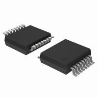
74LV4060DB,112 NXP Semiconductors, 74LV4060DB,112 Datasheet - Page 12

74LV4060DB,112
Manufacturer Part Number
74LV4060DB,112
Description
IC 14ST BINARY RIPPLE 16-SSOP
Manufacturer
NXP Semiconductors
Series
74LVr
Datasheet
1.74LV4060DB112.pdf
(18 pages)
Specifications of 74LV4060DB,112
Package / Case
16-SSOP
Logic Type
Binary Counter
Direction
Up
Number Of Elements
1
Number Of Bits Per Element
14
Reset
Asynchronous
Count Rate
90MHz
Trigger Type
Negative Edge
Voltage - Supply
1 V ~ 5.5 V
Operating Temperature
-40°C ~ 125°C
Mounting Type
Surface Mount
Counter Type
Binary Counters
Logic Family
74LV
Counting Method
Asynchronous
Operating Supply Voltage
1 V to 5.5 V
Operating Temperature Range
- 40 C to + 125 C
Mounting Style
SMD/SMT
Lead Free Status / RoHS Status
Lead free / RoHS Compliant
Timing
-
Lead Free Status / Rohs Status
Lead free / RoHS Compliant
Other names
568-2973-5
935166080112
935166080112
Philips Semiconductors
R2 is the power limiting resistor. For starting and maintaining
oscillation, a minimum transconductance is necessary, so R2 should
not be too large. A practical value for R2 is 2.2 kW.
Waveforms showing the clock (RS) to output (Q
delays, the clock pulse width, the output transition times and the
maximum clock frequency.
1998 Jun 23
14-stage binary ripple counter with oscillator
V
CP INPUT
GND
V
Q
V
I
OH
OL
n
C3
Figure 5. External components connection for
OUTPUT
22 to
37 pF
11
V
M
a typical crystal oscillator
t
RS
PHL
100 kW to 1 MW
MR (from logic)
1/
V
Figure 6.
f
M
R
max
bias
tW
C2
t
PLH
3
) propagation
R
10
R2
2.2 kW
TC
100 pF
SV00322
SV00326
12
1. V
2. V
Waveforms showing the master reset (MR) pulse width, the master
reset to output (Q
clock (RS) removal time.
Waveforms showing the output Q
delays.
NOTES:
Qn OUTPUT
V
the output load.
MR INPUT
RS INPUT
V
Q
V
V
Q
V
M
M
OL
OH
OL
OH
OL
n
n+1
OUTPUT
= 1.5 V at V
= 0.5
and V
GND
GND
GND
OUTPUT
V
CC
V
V
I
I
.
V
OH
CC
are the typical output voltage drop that occur with
n)
at V
CC
V
propagation delays and the master reset to
M
V
M
> 2.7 V and < 3.6 V
t
CC
PLH
t
PHL
< 2.7 V and > 4.5 V.
t
W
Figure 7.
Figure 8.
V
M
n
to output
V
M
t
rem
n + 1
Product specification
74LV4060
V
t
propagation
PHL
M
SV00329
SV00327


