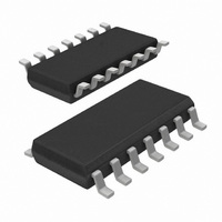
74LV393D,118 NXP Semiconductors, 74LV393D,118 Datasheet - Page 2

74LV393D,118
Manufacturer Part Number
74LV393D,118
Description
IC DUAL 4BIT BIN RIPPLE 14SOIC
Manufacturer
NXP Semiconductors
Series
74LVr
Datasheet
1.74LV393D112.pdf
(12 pages)
Specifications of 74LV393D,118
Package / Case
14-SOIC (3.9mm Width), 14-SOL
Logic Type
Binary Counter
Direction
Up
Number Of Elements
2
Number Of Bits Per Element
4
Reset
Asynchronous
Count Rate
20MHz
Trigger Type
Negative Edge
Voltage - Supply
1 V ~ 3.6 V
Operating Temperature
-40°C ~ 125°C
Mounting Type
Surface Mount
Counter Type
Binary Counters
Logic Family
74LV
Number Of Bits
4
Operating Supply Voltage
1 V to 5.5 V
Operating Temperature Range
- 40 C to + 125 C
Mounting Style
SMD/SMT
Lead Free Status / RoHS Status
Lead free / RoHS Compliant
Timing
-
Lead Free Status / Rohs Status
Lead free / RoHS Compliant
Other names
74LV393D-T
74LV393D-T
935162810118
74LV393D-T
935162810118
1. C
Philips Semiconductors
FEATURES
QUICK REFERENCE DATA
GND = 0V; T
NOTE:
ORDERING INFORMATION
PIN CONFIGURATION
t
f
C
C
14-Pin Plastic DIL
14-Pin Plastic SO
14-Pin Plastic SSOP Type II
14-Pin Plastic TSSOP Type I
1998 Jun 10
PHL
max
Optimized for Low Voltage applications: 1.0 to 3.6V
Accepts TTL input levels between V
Typical V
T
Typical V
T
Two 4-bit binary counters with individual clocks
Divide-by any binary module up to 28 in one package
Two master resets to clear each 4-bit counter individually
Output capability: standard
I
Dual 4-bit binary ripple counter
I
PD
CC
P
f
f
S (C
amb
amb
i
o
PD
D
= input frequency in MHz; C
SYMBOL
/t
= output frequency in MHz; V
category: MSI
PLH
= C
= 25 C
= 25 C
L
is used to determine the dynamic power dissipation (P
PD
OLP
OHV
V
amb
PACKAGES
CC
(output ground bounce) t 0.8V @ V
(output V
V
2
= 25 C; t
CC
GND
1MR
1CP
1Q
1Q
1Q
1Q
2
f
0
1
2
3
Propagation delay
nCP to nQ
nQ to nQn+1
nMR to nQn
Maximum clock frequency
Input capacitance
Power dissipation capacitance per flip-flop
o
) = sum of the outputs.
OH
f
1
2
3
4
5
6
7
r
i
)S (C
= t
undershoot) u 2V @ V
f
v2.5 ns
0
L
L
= output load capacity in pF;
CC
PARAMETER
CC
V
= supply voltage in V;
TEMPERATURE RANGE
CC
= 2.7V and V
2
SV00672
14
13
12
10
–40 C to +125 C
–40 C to +125 C
–40 C to +125 C
–40 C to +125 C
11
9
8
f
o
V
2CP
2MR
2Q
2Q
2Q
2Q
) where:
CC
0
1
2
3
CC
CC
CC
= 3.3V,
= 3.3V,
= 3.6V
D
in W)
C
V
V
OUTSIDE NORTH AMERICA
CC
I
L
= GND to V
= 15pF
2
= 3.3V
DESCRIPTION
The 74LV393 is a low–voltage Si-gate CMOS device and is pin and
function compatible with 74HC/HCT393.
The 74LV393 is a dual 4-bit binary ripple counter with separate
clocks (1CP, 2CP) and master reset (1MR, 2MR) inputs to each
counter.
The operation of each half of the ‘‘393’’ is the same as the ‘‘93’’
except no external clock connections are required. The counters are
triggered by a HIGH-to-LOW transition of the clock inputs. The
counter outputs are internally connected to provide clock inputs to
succeeding stages. The outputs of the ripple counter do not change
synchronously and should not be used for high-speed address
decoding.
The master resets are active-HIGH asynchronous inputs to each
4-bit counter identified by the ‘‘1’’ and ‘‘2’’ in the pin description.
A HIGH level on the nMR input overrides the clock and sets the
outputs LOW.
PIN DESCRIPTION
74LV393 PW
1, 13
2, 12
3, 4, 5, 6
11, 10, 9, 8
7
14
74LV393 DB
CONDITIONS
74LV393 N
74LV393 D
NUMBER
PIN
CC
1
1CP, 2CP
1MR, 2MR
1Q
2Q
GND
V
SYMBOL
CC
0
0
to 1Q
to 2Q
NORTH AMERICA
3
3
74LV393PW DH
74LV393 DB
74LV393 N
74LV393 D
Clock inputs
(HIGH-to-LOW, edge-triggered)
Asynchronous master reset inputs
(active HIGH)
Flip-flop outputs
Ground (0V)
Positive supply voltage
TYPICAL
3.5
12
99
23
11
4
FUNCTION
Product specification
74LV393
853–1936 19545
PKG. DWG. #
SOT108-1
SOT337-1
SOT402-1
SOT27-1
UNIT
MHz
ns
pF
pF


