74LV4020D,118 NXP Semiconductors, 74LV4020D,118 Datasheet
74LV4020D,118
Specifications of 74LV4020D,118
74LV4020D-T
935202700118


Related parts for 74LV4020D,118


74LV4020D,118 Summary of contents
Page 1
Rev. 01 — 29 November 2005 1. General description The 74LV4020 is a low-voltage Si-gate CMOS device and is pin and function compatible with the 74HC4020 and 74HCT4020. The 74LV4020 is a 14-stage binary ripple ...
Page 2
Philips Semiconductors 4. Quick reference data Table 1: GND = Symbol Parameter t , PHL t PLH t PHL f max [ input frequency in ...
Page 3
Philips Semiconductors 6. Functional diagram Fig 1. Functional diagram Fig 2. Logic symbol Fig 4. Logic diagram 74LV4020_1 Product data sheet ...
Page 4
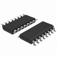
Philips Semiconductors 7. Pinning information 7.1 Pinning Fig 5. Pin configuration DIP16, SO16, SSOP16 and TSSOP16 7.2 Pin description Table 3: Symbol Q11 Q12 Q13 GND Q10 V CC 74LV4020_1 ...
Page 5
Philips Semiconductors 8. Functional description 8.1 Function table Table 4: Input HIGH voltage level LOW voltage level don’t care; = LOW-to-HIGH clock transition; = HIGH-to-LOW clock transition. 8.1.1 Timing diagram CP ...
Page 6
Philips Semiconductors 9. Limiting values Table 5: In accordance with the Absolute Maximum Rating System (IEC 60134). Voltages are referenced to GND (ground = 0 V). Symbol GND T ...
Page 7
Philips Semiconductors 11. Static characteristics Table 7: Static characteristics At recommended operating conditions; voltages are referenced to GND (ground = 0 V). Symbol Parameter [ +85 C amb V HIGH-state input voltage IH V LOW-state ...
Page 8
Philips Semiconductors Table 7: Static characteristics At recommended operating conditions; voltages are referenced to GND (ground = 0 V). Symbol Parameter V LOW-state input voltage IL V HIGH-state output voltage OH V LOW-state output voltage OL I input leakage current ...
Page 9
Philips Semiconductors 12. Dynamic characteristics Table 8: Dynamic characteristics Voltages are referenced to GND (ground = 0 V); C Symbol Parameter [ +85 C amb t , propagation delay PHL t PLH ...
Page 10
Philips Semiconductors Table 8: Dynamic characteristics Voltages are referenced to GND (ground = 0 V); C Symbol Parameter t recovery time rec maximum input clock frequency max C power dissipation capacitance ...
Page 11
Philips Semiconductors Table 8: Dynamic characteristics Voltages are referenced to GND (ground = 0 V); C Symbol Parameter t pulse width W CP (HIGH and LOW) MR (HIGH) t recovery time rec maximum input clock frequency ...
Page 12
Philips Semiconductors 13. Waveforms Fig 7. Propagation delay clock (CP) to output (Qn), clock pulse width and maximum clock Fig 8. Propagation delay master reset (MR) to output (Qn), pulse width master reset (MR) 74LV4020_1 Product data sheet V I ...
Page 13
Philips Semiconductors Fig 9. Load circuitry for switching times Table 9: Supply voltage V CC 1.2 V 2.0 V 2 3 5.5 V 74LV4020_1 Product data sheet V I PULSE GENERATOR Test ...
Page 14
Philips Semiconductors 14. Package outline DIP16: plastic dual in-line package; 16 leads (300 mil pin 1 index 1 DIMENSIONS (inch dimensions are derived from the original mm dimensions UNIT max. min. max. ...
Page 15
Philips Semiconductors SO16: plastic small outline package; 16 leads; body width 3 pin 1 index 1 DIMENSIONS (inch dimensions are derived from the original mm dimensions) A UNIT max. 0.25 ...
Page 16
Philips Semiconductors SSOP16: plastic shrink small outline package; 16 leads; body width 5 pin 1 index 1 e DIMENSIONS (mm are the original dimensions) A UNIT max. 0.21 1.80 mm ...
Page 17
Philips Semiconductors TSSOP16: plastic thin shrink small outline package; 16 leads; body width 4 pin 1 index 1 DIMENSIONS (mm are the original dimensions) A UNIT max. 0.15 0.95 mm ...
Page 18
Philips Semiconductors 15. Abbreviations Table 10: Abbreviations Acronym Description CMOS Complementary Metal Oxide Semiconductor TTL Transistor Transistor Logic HBM Human Body Model ESD ElectroStatic Discharge MM Machine Model 16. Revision history Table 11: Revision history Document ID Release date 74LV4020_1 ...
Page 19
Philips Semiconductors 17. Data sheet status [1] Level Data sheet status Product status I Objective data Development II Preliminary data Qualification III Product data Production [1] Please consult the most recently issued data sheet before initiating or completing a design. ...
Page 20
Philips Semiconductors 22. Contents 1 General description . . . . . . . . . . . . . . . . . . . . . . 1 2 Features . . . . . . . . ...