CY7C4261-15JC Cypress Semiconductor Corp, CY7C4261-15JC Datasheet
CY7C4261-15JC
Specifications of CY7C4261-15JC
Available stocks


Related parts for CY7C4261-15JC


CY7C4261-15JC Summary of contents
Page 1
... FIFO on each WCLK cycle. The output port is controlled in a similar manner by a free-running read clock (RCLK) and two read enable pins (REN1, REN2). In addition, the CY7C4261/71 has an output enable pin (OE). The read (RCLK) and write (WCLK) clocks may be tied together for single-clock operation or the two clocks may be run independently for asynchronous read/write applications ...
Page 2
... Functional Description (continued) The CY7C4261/71 provides four status pins: Empty, Full, Programmable Almost Empty, and Programmable Almost Full. The Almost Empty/Almost Full flags are programmable to single word granularity. The programmable flags default to Empty+7 and Full–7. The flags are synchronous, i.e., they change state relative to either the read clock (RCLK) or the write clock (WCLK) ...
Page 3
... Density 16K × 9 Package 32-pin PLCC,TQFP Architecture The CY7C4261/71 consists of an array of 16K to 32K words of nine bits each (implemented by a dual-port array of SRAM cells), a read pointer, a write pointer, control signals (RCLK, WCLK, REN1, REN2, WEN1, WEN2, RS), and flags (EF, PAE, PAF, FF). ...
Page 4
... FF). The partial status flags (PAE and PAF) can be detected from any one device. Figure 2 demonstrates a 18-bit word width by using two CY7C4261/71s. Any word width can be attained by adding additional CY7C4261/71s. When the CY7C4261/ Width-Expansion Configu- ration, the Read Enable (REN2) control input can be grounded (see Figure 2) ...
Page 5
... Figure 2. Block Diagram of 16K × 18/32K × 18 Deep Sync FIFO Memory Used in a Width-Expansion Configuration Document #: 38-06015 Rev. *B RESET (RS) 9 CY7C4261/ Read Enable 2 (REN2) CY7C4261 CY7C4271 READ CLOCK (RCLK) READ ENABLE 1 (REN1) OUTPUT ENABLE (OE) PROGRAMMABLE(PAE) EMPTY FLAG (EF) #1 EMPTY FLAG (EF DATA OUT (Q) ...
Page 6
... V < Com’l 35 Ind/Mil 40 Com’l 10 Ind/Mil 15 Description Test Conditions MHz 5.0V CC [10, 11] 3.0V GND R2 680 1.91V . OHZ CY7C4261 CY7C4271 Ambient Temperature + +125 C Min. Max. Min. Max. Min. 2.4 2.4 2.4 0.4 0.4 2.0 V 2 2.2 V 2.2 V 2.2 ...
Page 7
... Notes: 12. Pulse widths less than minimum values are not allowed. 13. Values guaranteed by design, not currently tested. Document #: 38-06015 Rev. *B 7C4261/71 10 7C4261/71 15 7C4261/71 25 7C4261/71 35 Min. Max. Min. 100 4 [13 [13 CY7C4261 CY7C4271 Max. Min. Max. Min. Max. 66.7 40 28.6 MHz ...
Page 8
... CLKL t ENH NO OPERATION t REF [15] t SKEW1 , then FF may not change state until the next WCLK rising edge. SKEW1 , then EF may not change state until the next RCLK rising edge. SKEW2 CY7C4261 CY7C4271 ENH NO OPERATION NO OPERATION t WFF t REF VALID DATA t OHZ Page ...
Page 9
... The first word is available the cycle after EF goes HIGH, always. Document #: 38-06015 Rev RSS t RSS t RSS t RSF t RSF t RSF D 1 [19] t FRL t SKEW1 t REF t OLZ t OE (maximum When t < minimum specification, t CLK SKEW2 SKEW2 CY7C4261 CY7C4271 t RSR t RSR t RSR [17 OE [20 (maximum) = either 2 FRL CLK SKEW1 Page ...
Page 10
... REN2 LOW OE Q –Q DATA IN OUTPUT REGISTER 0 8 Document #: 38-06015 Rev. *B [19 REF REF DATA WRITE t WFF t ENH t A DATA READ CY7C4261 CY7C4271 t DS DATA WRITE 2 t ENH t ENS t t ENH ENS [19] t FRL t t SKEW1 DATA READ NO WRITE [14] t SKEW1 t t ...
Page 11
... If a write is performed on this rising edge of the write clock, there will be Full 25. PAF offset = m. 26. 16,384 m words for CY7C4261, 32,768 27 the minimum time between a rising RCLK edge and a rising WCLK edge for PAF to change during that clock cycle. If the time between the rising edge of RCLK and ...
Page 12
... WEN2/LD t ENS REN1, REN2 Q – Document #: 38-06015 Rev CLKL t ENH PAE OFFSET PAE OFFSET LSB MSB t CLKL t ENH t A UNKNOWN PAE OFFSET LSB CY7C4261 CY7C4271 PAF OFFSET PAF OFFSET LSB MSB PAF OFFSET MSB PAF OFFSET PAE OFFSET MSB LSB Page ...
Page 13
... MHz 0.60 4.00 4.50 5.00 5.50 SUPPLY VOLTAGE (V) Ordering Information 16Kx9 Deep Sync FIFO Speed (ns) Ordering Code 10 CY7C4261-10AC CY7C4261-10JC CY7C4261-10AI CY7C4261-10JI 15 CY7C4261-15AC CY7C4261-15JC CY7C4261-15AI CY7C4261-15JI 25 CY7C4261-25AC CY7C4261-25JC CY7C4261-25AI CY7C4261-25JI Document #: 38-06015 Rev. *B vs. SUPPLY A 1.60 1.40 1.20 1.00 T =25 C 0.80 A 0.60 4 ...
Page 14
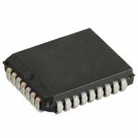
... J65 32-Lead Plastic Leaded Chip Carrier A32 32-Lead Thin Quad Flatpack J65 32-Lead Plastic Leaded Chip Carrier A32 32-Lead Thin Quad Flatpack J65 32-Lead Plastic Leaded Chip Carrier Subgroups CY7C4261 CY7C4271 Package Operating Type Range Commercial Industrial Package Operating Type Range ...
Page 15
... REF t 9, 10, 11 RFF t 9, 10, 11 WEF t 9, 10, 11 WFF t 9, 10, 11 WHF t 9, 10, 11 RHF t 9, 10, 11 RAE t 9, 10, 11 RPE t 9, 10, 11 WAF t 9, 10, 11 WPF t 9, 10, 11 XOL t 9, 10, 11 XOH Document #: 38-06015 Rev. *B Subgroups CY7C4261 CY7C4271 Page ...
Page 16
... Package Diagrams 32-Lead Thin Plastic Quad Flatpack 7 × 7 × 1.0 mm A32 Document #: 38-06015 Rev. *B 32-Lead Plastic Leaded Chip Carrier J65 CY7C4261 CY7C4271 51-85063-*B 51-85002-*B Page ...
Page 17
... Package Diagrams (continued) All product and company names mentioned in this document are the trademarks of their respective holders. Document #: 38-06015 Rev. *B 32-Pin Rectangular Leadless Chip Carrier L55 MIL-STD-1835 C-12 CY7C4261 CY7C4271 51-80068-** Page ...
Page 18
... Document History Page Document Title: CY7C4261, CY7C4271 16K/32K X 9 Deep Synchronous FIFOs Document Number: 38-06015 REV. ECN NO. Issue Date ** 106476 09/10/01 *A 122267 12/26/02 *B 127853 08/22/03 Document #: 38-06015 Rev. *B Orig. of Change SZV Changed from Spec number: 38-00658 to 38-06015 RBI Added power-up requirements Maximum Ratings Information ...