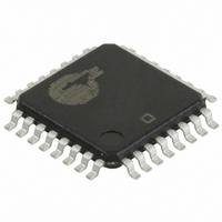
CY7C4241V-25AXC Cypress Semiconductor Corp, CY7C4241V-25AXC Datasheet - Page 4

CY7C4241V-25AXC
Manufacturer Part Number
CY7C4241V-25AXC
Description
IC SYNC FIFO MEM 4KX9 32-TQFP
Manufacturer
Cypress Semiconductor Corp
Series
CY7Cr
Datasheet
1.CY7C4241V-15AXC.pdf
(18 pages)
Specifications of CY7C4241V-25AXC
Function
Synchronous
Memory Size
36K (4K x 9)
Data Rate
100MHz
Access Time
15ns
Voltage - Supply
3.3V
Operating Temperature
-40°C ~ 85°C
Mounting Type
Surface Mount
Package / Case
32-TQFP
Lead Free Status / RoHS Status
Lead free / RoHS Compliant
Available stocks
Company
Part Number
Manufacturer
Quantity
Price
Company:
Part Number:
CY7C4241V-25AXC
Manufacturer:
Cypress Semiconductor Corp
Quantity:
10 000
Company:
Part Number:
CY7C4241V-25AXCT
Manufacturer:
Cypress Semiconductor Corp
Quantity:
10 000
Document #: 38-06010 Rev. *B
Programmable Flag (PAE, PAF) Operation
Whether the flag offset registers are programmed as
described in Table 1 or the default values are used, the
programmable Almost Empty Flag (PAE) and programmable
Almost Full Flag (PAF) states are determined by their corre-
sponding offset registers and the difference between the read
and write pointers.
Table 1. Writing the Offset Registers
Note:
1. The same selection sequence applies to reading from the registers. REN1 and REN2 are enabled and a read is performed on the LOW-to-HIGH transition of RCLK.
LD
0
0
1
1
8
8
8
8
WEN
64 x 9
0
1
0
1
6
6
Empty Offset (LSB) Reg.
Default Value = 007h
Full Offset (LSB) Reg
Default Value = 007h
WCLK
8
8
8
8
[1]
Empty Offset (LSB) Reg.
Default Value = 007h
Full Offset (LSB) Reg
Default Value = 007h
7
7
2K x 9
0
0
0
0
Empty Offset (LSB)
Empty Offset (MSB)
Full Offset (LSB)
Full Offset (MSB)
No Operation
Write Into FIFO
No Operation
2
2
(MSB)
(MSB)
000
000
8
8
8
8
Figure 1. Offset Register Location and Default Values
256 x 9
Selection
Empty Offset (LSB) Reg.
Default Value = 007h
7
7
Full Offset (LSB) Reg
Default Value = 007h
0
0
0
0
8
8
8
8
Empty Offset (LSB) Reg.
Default Value = 007h
Full Offset (LSB) Reg
Default Value = 007h
7
7
0
0
0
0
4K x 9
3
3
(MSB)
(MSB)
0000
0000
8
8
8
8
The number formed by the empty offset least significant bit
register and empty offset most significant register is referred
to as n and determines the operation of PAE. PAE is synchro-
nized to the LOW-to-HIGH transition of RCLK by one flip-flop
and is LOW when the FIFO contains n or fewer unread words.
PAE is set HIGH by the LOW-to-HIGH transition of RCLK
when the FIFO contains (n+1) or greater unread words.
The number formed by the full offset least significant bit
register and full offset most significant bit register is referred to
as m and determines the operation of PAF. PAE is synchro-
nized to the LOW-to-HIGH transition of WCLK by one flip-flop
and is set LOW when the number of unread words in the FIFO
is greater than or equal to CY7C4421V (64 – m), CY7C4201V
(256 – m), CY7C4211V (512 – m), CY7C4221V (1K – m),
CY7C4231V (2K – m), CY7C4241V (4K – m), and
CY7C4251V (8K – m). PAF is set HIGH by the LOW-to-HIGH
transition of WCLK when the number of available memory
locations is greater than m.
512 x 9
Empty Offset (LSB) Reg.
Default Value = 007h
Full Offset (LSB) Reg
Default Value = 007h
7
7
CY7C4421V/4201V/4211V/4221V
0
0
0
0
8
8
8
8
CY7C4231V/4241V/4251V
(MSB)
(MSB)
0
0
0
0
0
0
Empty Offset (LSB) Reg.
Default Value = 007h
Full Offset (LSB) Reg
Default Value = 007h
7
7
8K x 9
4
4
8
8
8
8
(MSB)
00000
(MSB)
00000
Empty Offset (LSB) Reg.
Default Value = 007h
Full Offset (LSB) Reg
Default Value = 007h
1K x 9
7
7
0
0
0
0
1
1
(MSB)
(MSB)
00
00
Page 4 of 18
0
0
0
0


