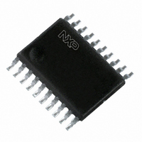
74LVC374APW,118 NXP Semiconductors, 74LVC374APW,118 Datasheet - Page 6

74LVC374APW,118
Manufacturer Part Number
74LVC374APW,118
Description
IC OCT D FF POS-EDG TRIG 20TSSOP
Manufacturer
NXP Semiconductors
Series
74LVCr
Type
D-Type Busr
Datasheet
1.74LVC374APW118.pdf
(24 pages)
Specifications of 74LVC374APW,118
Package / Case
20-TSSOP
Function
Standard
Output Type
Tri-State Non Inverted
Number Of Elements
1
Number Of Bits Per Element
8
Frequency - Clock
80MHz
Delay Time - Propagation
1.5ns
Trigger Type
Positive Edge
Current - Output High, Low
24mA, 24mA
Voltage - Supply
2.7 V ~ 3.6 V
Operating Temperature
-40°C ~ 125°C
Mounting Type
Surface Mount
Number Of Circuits
1
Logic Family
LVC
Logic Type
D-Type Edge Triggered Flip-Flop
Polarity
Non-Inverting
Input Type
Single-Ended
Propagation Delay Time
2.7 ns at 3.3 V
High Level Output Current
- 24 mA
Supply Voltage (max)
3.6 V
Maximum Operating Temperature
+ 125 C
Mounting Style
SMD/SMT
Minimum Operating Temperature
- 40 C
Supply Voltage (min)
1.2 V
Lead Free Status / RoHS Status
Lead free / RoHS Compliant
Lead Free Status / RoHS Status
Lead free / RoHS Compliant, Lead free / RoHS Compliant
Other names
568-4499-2
74LVC374APW-T
74LVC374APW-T
935218680118
74LVC374APW-T
74LVC374APW-T
935218680118
Available stocks
Company
Part Number
Manufacturer
Quantity
Price
Company:
Part Number:
74LVC374APW,118
Manufacturer:
NXP Semiconductors
Quantity:
2 000
Philips Semiconductors
RECOMMENDED OPERATING CONDITIONS
LIMITING VALUES
In accordance with the Absolute Maximum Rating System (IEC 60134); voltages are referenced to GND (ground = 0 V).
Notes
1. The input and output voltage ratings may be exceeded if the input and output current ratings are observed.
2. For SO20 packages: above 70 C derate linearly with 8 mW/K.
2003 May 14
V
V
V
T
t
V
I
V
I
V
I
I
T
P
r
IK
OK
O
CC
SYMBOL
SYMBOL
, t
amb
stg
CC
I
O
CC
I
O
tot
Octal D-type flip-flop with 5 V tolerant inputs/outputs;
positive edge-trigger; 3-state
f
, I
For SSOP20 and TSSOP20 packages: above 60 C derate linearly with 5.5 mW/K.
For DHVQFN20 packages: above 60 C derate linearly with 4.5 mW/K.
GND
supply voltage
input voltage
output voltage
operating ambient temperature
input rise and fall times
supply voltage
input diode current
input voltage
output diode current
output voltage
output source or sink current
V
storage temperature
power dissipation
CC
or GND current
PARAMETER
PARAMETER
for maximum speed performance
for low-voltage applications
output HIGH or LOW state
output 3-state
in free air
V
V
V
note 1
V
output HIGH or LOW state; note 1
output 3-state; note 1
V
T
amb
CC
CC
I
O
O
< 0
> V
= 0 to V
= 1.2 to 2.7 V
= 2.7 to 3.6 V
= 40 to +125 C; note 2
CC
6
CONDITIONS
CONDITIONS
or V
CC
O
< 0
2.7
1.2
0
0
0
0
0
40
0.5
0.5
0.5
0.5
65
MIN.
MIN.
3.6
3.6
5.5
V
5.5
+125
20
10
+6.5
+6.5
V
+6.5
+150
500
Product specification
50
50
50
100
74LVC374A
CC
CC
MAX.
MAX.
+ 0.5 V
V
V
V
V
V
ns/V
ns/V
V
mA
V
mA
V
mA
mA
mW
C
C
UNIT
UNIT


