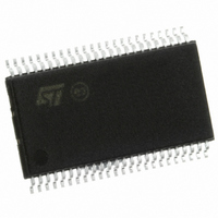
74VCX16374TTR STMicroelectronics, 74VCX16374TTR Datasheet

74VCX16374TTR
Specifications of 74VCX16374TTR
Related parts for 74VCX16374TTR
74VCX16374TTR Summary of contents
Page 1
... All inputs and outputs are equipped with protection circuits against static discharge, giving them 2KV ESD immunity and transient excess voltage. February 2003 = 3.0 to 3.6V = 2.3 to 2.7V = 1. 2.3V ORDER CODES CC = 1.8V CC PACKAGE TSSOP PIN CONNECTION 2 MOS 74VCX16374 TSSOP TUBE T & R 74VCX16374TTR 1/12 ...
Page 2
INPUT AND OUTPUT EQUIVALENT CIRCUIT PIN DESCRIPTION PIN No SYMBOL NAME AND FUNCTION 1 1OE 3 State Output Enable Input (Active LOW 1Q0 to 1Q7 3-State Outputs 11, 12 13, 14, 16, 17, ...
Page 3
LOGIC DIAGRAM This logic diagram has not to be used to estimate propagation delays ABSOLUTE MAXIMUM RATINGS Symbol V Supply Voltage Input Voltage Output Voltage (OFF State Output Voltage (High or ...
Page 4
DC SPECIFICATIONS (2.7V < V Symbol Parameter V High Level Input IH Voltage V Low Level Input IL Voltage V High Level Output OH Voltage V Low Level Output OL Voltage I Input Leakage I Current I Power Off ...
Page 5
DC SPECIFICATIONS (2.3V < V Symbol Parameter V High Level Input IH Voltage V Low Level Input IL Voltage V High Level Output OH Voltage V Low Level Output OL Voltage I Input Leakage I Current I Power Off Leakage ...
Page 6
DYNAMIC SWITCHING CHARACTERISTICS (T Symbol Parameter V Dynamic Low Voltage Quiet OLP Output (note Dynamic Low Voltage Quiet OLV Output (note Dynamic High Voltage Quiet OHV Output (note Number of ...
Page 7
CAPACITIVE CHARACTERISTICS Symbol Parameter C Input Capacitance IN C Output Capacitance OUT C Power Dissipation Capacitance PD (note defined as the value of the IC’s internal equivalent capacitance which is calculated from the operating current consumption ...
Page 8
WAVEFORM 1: nCK TO Qn PROPAGATION DELAYS, nCK MAXIMUM FREQUENCY nCK SETUP AND HOLD TIMES (f=1MHz; 50% duty cycle) WAVEFORM 2: OUTPUT ENABLE AND DISABLE TIME (f=1MHz; 50% duty cycle) 8/12 ...
Page 9
WAVEFORM 3 : nCK MINIMUM PULSE WIDTH (f=1MHz; 50% duty cycle) 74VCX16374 9/12 ...
Page 10
DIM. MIN 0. 0.17 c 0. 0˚ PIN 1 IDENTIFICATION 1 10/12 TSSOP48 MECHANICAL DATA mm. TYP MAX. 1.2 0.15 0.9 0.27 ...
Page 11
Tape & Reel TSSOP48 MECHANICAL DATA mm. DIM. MIN. TYP A C 12 8.7 Bo 13.1 Ko 1.5 Po 3.9 P 11.9 inch MAX. MIN. TYP. 330 13.2 0.504 0.795 2.362 30.4 8.9 0.343 ...
Page 12
... No license is granted by implication or otherwise under any patent or patent rights of STMicroelectronics. Specifications mentioned in this publication are subject to change without notice. This publication supersedes and replaces all information previously supplied ...


