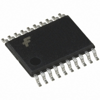
MM74HCT574MTC Fairchild Semiconductor, MM74HCT574MTC Datasheet - Page 4

MM74HCT574MTC
Manufacturer Part Number
MM74HCT574MTC
Description
IC FLIP FLOP OCT D 3ST 20-TSSOP
Manufacturer
Fairchild Semiconductor
Series
74HCTr
Type
D-Type Busr
Datasheet
1.MM74HCT574MTC.pdf
(9 pages)
Specifications of MM74HCT574MTC
Function
Standard
Output Type
Tri-State Non Inverted
Number Of Elements
1
Number Of Bits Per Element
8
Frequency - Clock
33MHz
Delay Time - Propagation
18ns
Trigger Type
Positive Edge
Current - Output High, Low
7.2mA, 7.2mA
Voltage - Supply
4.5 V ~ 5.5 V
Operating Temperature
-40°C ~ 85°C
Mounting Type
Surface Mount
Package / Case
20-TSSOP
Logic Family
HCT
Technology
CMOS
Number Of Bits
8
Number Of Elements
1
Clock-edge Trigger Type
Positive-Edge
Polarity
Non-Inverting
Operating Supply Voltage (typ)
5V
Package Type
TSSOP
Propagation Delay Time
38ns
Low Level Output Current
7.2mA
High Level Output Current
-7.2mA
Frequency (max)
28MHz
Operating Supply Voltage (min)
4.5V
Operating Supply Voltage (max)
5.5V
Operating Temp Range
-40C to 85C
Operating Temperature Classification
Industrial
Mounting
Surface Mount
Pin Count
20
Lead Free Status / RoHS Status
Lead free / RoHS Compliant
www.fairchildsemi.com
t
t
t
t
t
t
t
t
t
t
t
t
t
t
t
t
t
t
t
t
t
t
t
t
C
C
C
PHL
PLH
PHL
PLH
PZH
PZL
PHZ
PLZ
W
S
H
PHL
PLH
PHL
PLH
PZH
PZL
PHZ
PLZ
THL
TLH
W
S
H
AC Electrical Characteristics
AC Electrical Characteristics
V
Note 5: C
I
V
S
Symbol
IN
OUT
PD
Symbol
CC
CC
C
PD
5.0V
5.0V, t
V
PD
CC
determines the no load dynamic power consumption, P
Maximum Propagation Delay
Data to Output
Maximum Propagation Delay
Latch Enable to Output
Maximum Enable Propagation Delay C
Control to Output
Maximum Disable Propagation Delay C
Control to Output
Minimum Clock Pulse Width
Minimum Setup Time Data to Clock
Minimum Hold Time Clock to Data
Maximum Propagation
Delay Data to Output
Maximum Propagation Delay
Latch Enable to Output
Maximum Enable Propagation
Delay Control to Output
Maximum Disable Propagation
Delay Control to Output
Maximum Output
Rise and Fall Time
Minimum Clock Pulse Width
Minimum Setup Time Data to Clock
Minimum Hold Time Clock to Data
Maximum Input Capacitance
Maximum Output Capacitance
Power Dissipation Capacitance
(Note 5)
f
r
I
10%, t
CC
r
.
t
f
r
6 ns, T
Parameter
Parameter
t
f
6 ns (unless otherwise specified)
A
25
q
C (unless otherwise specified)
C
C
C
R
C
R
C
OC
OC
C
C
R
R
L
L
L
L
L
L
L
L
L
L
L
L
L
Conditions
50 pF
50 pF
50 pF
1 k
50 pF
1 k
50 pF
V
GND
45 pF
45 pF
45 pF
1 k
5 pF
1 k
CC
MM74HCT573
MM74HCT573
:
:
:
:
Conditions
D
C
PD
V
CC
4
2 f
Typ
18
17
22
15
6
4
I
3
CC
T
A
V
CC
25
, and the no load dynamic current consumption,
q
30
30
30
30
12
15
12
10
20
52
5
5
Typ
17
16
21
14
T
A
Guaranteed Limits
40 to 85
38
44
38
38
15
20
15
10
20
6
Guaranteed Limit
q
C T
27
27
30
23
15
12
5
A
55 to 125
45
53
45
45
18
24
18
10
20
8
q
C
Units
ns
ns
ns
ns
ns
ns
ns
Units
ns
ns
ns
ns
ns
ns
ns
ns
pF
pF
pF


