74LV574DB,112 NXP Semiconductors, 74LV574DB,112 Datasheet
74LV574DB,112
Specifications of 74LV574DB,112
74LV574DB
935152950112


Related parts for 74LV574DB,112


74LV574DB,112 Summary of contents
Page 1
Octal D-type flip-flop; positive edge-trigger; 3-state Rev. 04 — 14 May 2009 1. General description The 74LV574 is an octal D-type flip–flop featuring separate D-type inputs for each flip-flop and non-inverting 3-state outputs for bus oriented applications. A clock ...
Page 2
... NXP Semiconductors 4. Functional diagram Fig 1. Logic symbol Fig 3. Functional diagram 74LV574_4 Product data sheet Octal D-type flip-flop; positive edge-trigger; 3-state mna798 Fig FF1 3-STATE OUTPUTS FF8 Rev. 04 — 14 May 2009 74LV574 mna446 IEC logic symbol mna800 © NXP B.V. 2009. All rights reserved. ...
Page 3
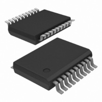
... NXP Semiconductors FF1 FF2 Fig 4. Logic diagram 5. Pinning information 5.1 Pinning 74LV574 GND 10 001aaj968 Fig 5. Pin configuration DIP20, SO20 5.2 Pin description Table 2. Pin description Symbol Pin GND 19, 18, 17, 16, 15, 14, 13 74LV574_4 Product data sheet Octal D-type flip-flop; positive edge-trigger; 3-state ...
Page 4
... NXP Semiconductors 6. Functional description [1] Table 3. Function table Operating mode Input OE Load and read register L L Load register and disable H outputs H [ HIGH voltage level h = HIGH voltage level one set-up time prior to the LOW to HIGH CP transition L = LOW voltage level l = LOW voltage level one set-up time prior to the LOW to HIGH CP transition ...
Page 5
... NXP Semiconductors 8. Recommended operating conditions Table 5. Recommended operating conditions Voltages are referenced to GND (ground = 0 V). Symbol Parameter [1] V supply voltage CC V input voltage I V output voltage O T ambient temperature amb t/ V input transition rise and fall rate [1] The static characteristics are guaranteed from ...
Page 6
... NXP Semiconductors Table 6. Static characteristics At recommended operating conditions. Voltages are referenced to GND (ground = 0 V). Symbol Parameter V LOW-level output voltage OL I input leakage current I I OFF-state output current OZ I supply current CC I additional supply current CC C input capacitance I [1] Typical values are measured ...
Page 7
... NXP Semiconductors Table 7. Dynamic characteristics Voltages are referenced to GND (ground = 0 V). For test circuit see Symbol Parameter Conditions t disable time OE to Qn; dis pulse width CP, HIGH or LOW; see set-up time Dn to CP; see hold time Dn to CP; see maximum see max frequency power dissipation ...
Page 8
... NXP Semiconductors 11. Waveforms CP input Qn output Measurement points are given in V and V are typical output voltage levels that occur with the output load Fig 7. The clock (CP) to output (Qn) propagation delays, the clock pulse (CP) and the maximum clock pulse frequency OE input output LOW-to-OFF ...
Page 9
... NXP Semiconductors CP input Dn input Qn output Measurement points are given in The shaded areas indicate when the input is permitted to change for predictable output performance. V and V are typical output voltage levels that occur with the output load Fig 9. The data set-up and hold times for the Dn input to the CP input) Table 8 ...
Page 10
... NXP Semiconductors Test data is given in Table Definitions for test circuit Load resistance Load capacitance including jig and probe capacitance Termination resistance should be equal to output impedance External voltage for measuring switching times. EXT Fig 10. Test circuit for measuring switching times Table 9. Test data ...
Page 11
... NXP Semiconductors 12. Package outline DIP20: plastic dual in-line package; 20 leads (300 mil pin 1 index 1 DIMENSIONS (inch dimensions are derived from the original mm dimensions UNIT max. min. max. mm 4.2 0.51 3.2 inches 0.17 0.02 0.13 Note 1. Plastic or metal protrusions of 0.25 mm (0.01 inch) maximum per side are not included. ...
Page 12
... NXP Semiconductors SO20: plastic small outline package; 20 leads; body width 7 pin 1 index 1 e DIMENSIONS (inch dimensions are derived from the original mm dimensions) A UNIT max. 0.3 2.45 2.65 mm 0.25 0.1 2.25 0.012 0.096 0.1 inches 0.01 0.004 0.089 Note 1. Plastic or metal protrusions of 0.15 mm (0.006 inch) maximum per side are not included. ...
Page 13
... NXP Semiconductors SSOP20: plastic shrink small outline package; 20 leads; body width 5 pin 1 index 1 e DIMENSIONS (mm are the original dimensions) A UNIT max. 0.21 1. 0.25 0.05 1.65 Note 1. Plastic or metal protrusions of 0.2 mm maximum per side are not included. OUTLINE VERSION IEC SOT339-1 Fig 13. Package outline SOT339-1 (SSOP20) ...
Page 14
... NXP Semiconductors TSSOP20: plastic thin shrink small outline package; 20 leads; body width 4 pin 1 index 1 DIMENSIONS (mm are the original dimensions) A UNIT max. 0.15 0.95 mm 1.1 0.25 0.05 0.80 Notes 1. Plastic or metal protrusions of 0.15 mm maximum per side are not included. 2. Plastic interlead protrusions of 0.25 mm maximum per side are not included. ...
Page 15
... NXP Semiconductors 13. Abbreviations Table 10. Abbreviations Acronym Description CMOS Complementary Metal Oxide Semiconductor DUT Device Under Test ESD ElectroStatic Discharge HBM Human Body Model MM Machine Model TTL Transistor-Transistor Logic 14. Revision history Table 11. Revision history Document ID Release date 74LV574_4 20090514 • Modifications: ...
Page 16
... Right to make changes — NXP Semiconductors reserves the right to make changes to information published in this document, including without limitation specifications and product descriptions, at any time and without notice ...
Page 17
... NXP Semiconductors 17. Contents 1 General description . . . . . . . . . . . . . . . . . . . . . . 1 2 Features . . . . . . . . . . . . . . . . . . . . . . . . . . . . . . . 1 3 Ordering information . . . . . . . . . . . . . . . . . . . . . 1 4 Functional diagram . . . . . . . . . . . . . . . . . . . . . . 2 5 Pinning information . . . . . . . . . . . . . . . . . . . . . . 3 5.1 Pinning . . . . . . . . . . . . . . . . . . . . . . . . . . . . . . . 3 5.2 Pin description . . . . . . . . . . . . . . . . . . . . . . . . . 3 6 Functional description . . . . . . . . . . . . . . . . . . . 4 7 Limiting values Recommended operating conditions Static characteristics Dynamic characteristics . . . . . . . . . . . . . . . . . . 6 11 Waveforms . . . . . . . . . . . . . . . . . . . . . . . . . . . . . 8 12 Package outline . . . . . . . . . . . . . . . . . . . . . . . . 11 13 Abbreviations . . . . . . . . . . . . . . . . . . . . . . . . . . 15 14 Revision history ...