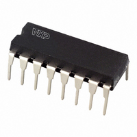
HEF40174BP,652 NXP Semiconductors, HEF40174BP,652 Datasheet - Page 2

HEF40174BP,652
Manufacturer Part Number
HEF40174BP,652
Description
IC HEX D-TYPE FLIP FLOP 16DIP
Manufacturer
NXP Semiconductors
Series
4000Br
Type
D-Type Busr
Specifications of HEF40174BP,652
Package / Case
16-DIP (0.300", 7.62mm)
Function
Master Reset
Output Type
Inverted
Number Of Elements
1
Number Of Bits Per Element
6
Frequency - Clock
45MHz
Delay Time - Propagation
20ns
Trigger Type
Positive Edge
Voltage - Supply
3 V ~ 15 V
Mounting Type
Through Hole
Number Of Circuits
1
Logic Family
HEF4000
Logic Type
D-Type Edge Triggered Flip-Flop
Polarity
Non-Inverting
Input Type
Single-Ended
Propagation Delay Time
20 ns at 15 V
High Level Output Current
- 3.6 mA
Low Level Output Current
3.6 mA
Supply Voltage (max)
15.5 V
Maximum Operating Temperature
+ 85 C
Mounting Style
SMD/SMT
Minimum Operating Temperature
- 40 C
Supply Voltage (min)
4.5 V
Lead Free Status / RoHS Status
Lead free / RoHS Compliant
Operating Temperature
-
Current - Output High, Low
-
Lead Free Status / Rohs Status
Lead free / RoHS Compliant
Other names
933296750652
HEF40174BPN
HEF40174BPN
HEF40174BPN
HEF40174BPN
Philips Semiconductors
DESCRIPTION
The HEF40174B is a hex edge-triggered D-type flip-flop
with six data inputs (D
overriding asynchronous master reset input (MR), and six
FAMILY DATA, I
See Family Specifications
January 1995
HEF40174BP(N): 16-lead DIL; plastic
HEF40174BD(F): 16-lead DIL; ceramic (cerdip)
HEF40174BT(D): 16-lead SO; plastic
( ): Package Designator North America
Hex D-type flip-flop
DD
Fig.2 Pinning diagram.
LIMITS category MSI
(SOT38-1)
(SOT74)
(SOT109-1)
0
to D
5
), a clock input (CP), an
Fig.1 Functional diagram.
2
buffered outputs (O
transferred to O
CP if MR is HIGH. When LOW, MR resets all flip-flops
(O
PINNING
FUNCTION TABLE
Notes
1. H = HIGH state (the more positive voltage)
D
CP
MR
O
0
0
0
L = LOW state (the less positive voltage)
X = state is immaterial
to O
to D
to O
CP
X
5
5
5
= positive-going transition
= negative-going transition
= LOW) independent of CP and D
data inputs
clock input (LOW to HIGH; edge-triggered)
master reset input (active LOW)
buffered outputs
0
INPUTS
to O
D
H
X
X
L
0
to O
5
on the LOW to HIGH transition of
5
). Information on D
MR
H
H
H
L
Product specification
HEF40174B
no change
0
OUTPUT
0
to D
to D
O
H
L
L
MSI
5
.
5
is


