NB4L52MNG ON Semiconductor, NB4L52MNG Datasheet
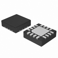
IC FLIP FLOP DATA/CLK DFF 16-QFN

NB4L52MNG

Manufacturer Part Number
NB4L52MNG
Description
IC FLIP FLOP DATA/CLK DFF 16-QFN
Manufacturer
ON Semiconductor
Type
D-Typer
Datasheet

Specifications of NB4L52MNG

Function
Reset
Output Type
Differential
Number Of Elements
1
Number Of Bits Per Element
1
Delay Time - Propagation
400ps
Trigger Type
Negative Edge
Voltage - Supply
2.3 V ~ 5.5 V
Operating Temperature
-40°C ~ 85°C
Mounting Type
Surface Mount
Package / Case
16-TQFN Exposed Pad
Logic Type
Registered Translator
Translation
CML/ECL/LVCMOS/LVDS/LVTTL to LVPECL
Propagation Delay Time
0.5 ns
Supply Voltage (max)
- 5.5 V, + 5.5 V
Supply Voltage (min)
- 2.375 V, + 2.375 V
Maximum Operating Temperature
+ 85 C
Minimum Operating Temperature
- 40 C
Mounting Style
SMD/SMT
Flip-flop Type
D
Propagation Delay
330ps
Frequency
4GHz
Output Current
25mA
Ic Output Type
Differential / Complementary
Supply Voltage Range
± 2.375V To ± 5.5V
Rohs Compliant
Yes
Lead Free Status / RoHS Status
Lead free / RoHS Compliant
Current - Output High, Low
-
Frequency - Clock
-
Lead Free Status / Rohs Status
Lead free / RoHS Compliant

Available stocks

Company
Part Number
Manufacturer
Quantity
Price
Part Number:
NB4L52MNG
Manufacturer:
ON
Quantity:
123
Part Number:
NB4L52MNG
Manufacturer:
ON Semiconductor
Quantity:
2
NB4L52
2.5 V/3.3 V/5.0 V Differential
Data/Clock D Flip-Flop
with Reset
Multi−Level Inputs to LVPECL Translator
w/ Internal Termination
differential asynchronous Reset. The differential inputs incorporate
internal 50 W termination resistors and will accept PECL, LVPECL,
LVCMOS, LVTTL, CML, or LVDS logic levels. When Clock
transitions from Low to High, Data will be transferred to the
differential LVPECL outputs. The differential Clock inputs allow the
NB4L52 to also be used as a negative edge triggered device. The
device is housed in a small 3x3 mm 16 pin QFN package.
Features
© Semiconductor Components Industries, LLC, 2009
August, 2009 − Rev. 3
The NB4L52 is a differential Data and Clock D flip−flop with a
LVEP, EP, and SG Devices
Maximum Input Clock Frequency > 4 GHz Typical
330 ps Typical Propagation Delay
145 ps Typical Rise and Fall Times
Differential LVPECL Outputs, 750 mV Peak−to−Peak, Typical
Operating Range: V
Internal Input Termination Resistors, 50 W
Functionally Compatible with Existing 2.5 V/3.3 V/5.0 V LVEL,
−40°C to +85°C Ambient Operating Temperature
These are Pb−Free Devices
CC
= 2.375 V to 5.5 V with V
EE
= 0 V
1
Table 1. TRUTH TABLE
Z = LOW to HIGH Transition
x = Don’t Care
See detailed ordering and shipping information in the package
dimensions section on page 7 of this data sheet.
*For additional marking information, refer to
Application Note AND8002/D.
R
H
L
L
CASE 485G
MN SUFFIX
(Note: Microdot may be in either location)
VTCLK
VTCLK
QFN−16
VTD
VTD
CLK
CLK
1
ORDERING INFORMATION
Figure 1. Logic Diagram
D
D
A
L
Y
W
G
http://onsemi.com
= Assembly Location
= Wafer Lot
= Year
= Work Week
= Pb−Free Package
D
H
x
L
VTR R
Data
Clock
MARKING DIAGRAM*
Publication Order Number:
1
Reset
CLK
16
Z
Z
x
R
ALYWG
NB4L
VTR
52
G
NB4L52/D
Q
H
L
L
Q
Q

Related parts for NB4L52MNG

NB4L52MNG Summary of contents

Page 1

NB4L52 2.5 V/3.3 V/5.0 V Differential Data/Clock D Flip-Flop with Reset Multi−Level Inputs to LVPECL Translator w/ Internal Termination The NB4L52 is a differential Data and Clock D flip−flop with a differential asynchronous Reset. The differential inputs incorporate internal 50 ...

Page 2

Table 2. PIN DESCRIPTION Pin Name I − ECL, CML, LVCMOS, LVDS, LVTTL Input 3 D ECL, CML, LVCMOS, LVDS, LVTTL Input 4 V − − TCLK 6 CLK ECL, CML, LVCMOS, ...

Page 3

Table 3. ATTRIBUTES ESD Protection Moisture Sensitivity (Note 2) Flammability Rating Oxygen Index Transistor Count Meets or exceeds JEDEC Spec EIA/JESD78 IC Latchup Test 2. For additional information, see Application Note AND8003/D. Table 4. MAXIMUM RATINGS Symbol ...

Page 4

Table 5. DC CHARACTERISTICS, CLOCK INPUTS, LVPECL OUTPUTS (V = 2.375 Symbol Characteristic I Power Supply Current (Inputs and Outputs Open Output HIGH Voltage (Note ...

Page 5

Table 6. AC CHARACTERISTICS V CC Symbol Characteristic V Output Voltage Amplitude (@ V OUTPP (Note 10) (See Figure Propagation Delay to PLH t Output Differential PHL t Setup Time s t Hold Time h t Reset ...

Page 6

CLK/D CLK/D Figure 4. Differential Input Driven Single−Ended Figure 6. Differential Inputs Driven Differentially IHmax V thmax V ILmax CLK IHmin V thmin V CLK ILmin ...

Page 7

... Q Figure 10. Typical Termination for Output Driver and Device Evaluation (See Application Note AND8020/D − Termination of ECL Logic Devices.) ORDERING INFORMATION Device Package NB4L52MNG QFN−16 (Pb−Free) NB4L52MNR2G QFN−16 (Pb−Free) †For information on tape and reel specifications, including part orientation and tape sizes, please refer to our Tape and Reel Packaging Specifications Brochure, BRD8011/D ...

Page 8

... E2 e 3.25 0.128 *For additional information on our Pb−Free strategy and soldering details, please download the ON Semiconductor Soldering and Mounting Techniques Reference Manual, SOLDERRM/D. 6,362,644. N. American Technical Support: 800−282−9855 Toll Free USA/Canada Europe, Middle East and Africa Technical Support: Phone: 421 33 790 2910 Japan Customer Focus Center Phone: 81− ...

Related keywords