DM74AS574N Fairchild Semiconductor, DM74AS574N Datasheet

IC F/F OCTAL D-TYPE 3ST 20-DIP

DM74AS574N

Manufacturer Part Number
DM74AS574N
Description
IC F/F OCTAL D-TYPE 3ST 20-DIP
Manufacturer
Fairchild Semiconductor
Series
74ASr
Type
D-Type Busr
Datasheet

Specifications of DM74AS574N

Function
Standard
Output Type
Tri-State Non Inverted
Number Of Elements
1
Number Of Bits Per Element
8
Frequency - Clock
80MHz
Delay Time - Propagation
3ns
Trigger Type
Positive Edge
Current - Output High, Low
15mA, 48mA
Voltage - Supply
4.5 V ~ 5.5 V
Operating Temperature
0°C ~ 70°C
Mounting Type
Through Hole
Package / Case
20-DIP (0.300", 7.62mm)
Logic Family
AS
Technology
Bipolar
Number Of Bits
8
Number Of Elements
1
Clock-edge Trigger Type
Positive-Edge
Polarity
Non-Inverting
Operating Supply Voltage (typ)
5V
Package Type
DIP
Propagation Delay Time
10ns
Low Level Output Current
48mA
High Level Output Current
-15mA
Frequency (max)
80MHz
Operating Supply Voltage (min)
4.5V
Operating Supply Voltage (max)
5.5V
Operating Temp Range
0C to 70C
Operating Temperature Classification
Commercial
Mounting
Through Hole
Pin Count
20
Lead Free Status / RoHS Status
Lead free / RoHS Compliant
Other names
74AS574
© 2000 Fairchild Semiconductor Corporation
DM74AS574WM
DM74AS574N
DM74AS574
Octal D-Type Edge-Triggered Flip-Flops
with 3-STATE Outputs
General Description
These 8-bit registers feature totem-pole 3-STATE outputs
designed specifically for driving highly-capacitive or rela-
tively low-impedance loads. The high-impedance state and
increased HIGH-logic-level drive provide these registers
with the capability of being connected directly to and driv-
ing the bus lines in a bus-organized system without need
for interface or pull-up components. They are particularly
attractive for implementing buffer registers, I/O ports, bidi-
rectional bus drivers, and working registers.
The eight flip-flops of the DM74AS574 are edge-triggered
D-type flip-flops. On the positive transition of the clock, the
Q outputs will be set to the logic states that were set up at
the D inputs.
A buffered output control input can be used to place the
eight outputs in either a normal logic state (HIGH or LOW
logic levels) or a high impedance state. In the high-imped-
ance state the outputs neither load nor drive the bus lines
significantly.
The output control does not affect the internal operation of
the flip-flops. That is, the old data can be retained or new
data can be entered even while the outputs are OFF.
The pinout is arranged to ease printed circuit board layout.
All data inputs are on one side of the package while all the
outputs are on the other side.
Ordering Code:
Devices also available in Tape and Reel. Specify by appending the suffix letter “X” to the ordering code.
Connection Diagram
Order Number
Package Number
M20B
N20A
20-Lead Small Outline Integrated Circuit (SOIC), JEDEC MS-013, 0.300 Wide
20-Lead Plastic Dual-In-Line Package (PDIP), JEDEC MS-001, 0.300 Wide
DS006314
Features
Switching specifications at 50 pF
Switching specifications guaranteed over full tempera-
ture and V
Advanced oxide-isolated, ion-implanted Schottky TTL
process
Functionally equivalent with DM74S374
Improved AC performance over DM74S374 at approxi-
mately half the power
3-STATE buffer-type outputs drive bus lines directly
Bus structured pinout
Package Description
CC
range
October 1986
Revised March 2000
www.fairchildsemi.com

Related parts for DM74AS574N

DM74AS574N Summary of contents

Page 1

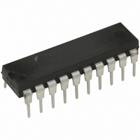
... Package Number DM74AS574WM M20B 20-Lead Small Outline Integrated Circuit (SOIC), JEDEC MS-013, 0.300 Wide DM74AS574N N20A 20-Lead Plastic Dual-In-Line Package (PDIP), JEDEC MS-001, 0.300 Wide Devices also available in Tape and Reel. Specify by appending the suffix letter “X” to the ordering code. ...

Page 2

Function Table Output Clock D Control LOW State H HIGH State X Don’t Care Positive Edge Transition Z High Impedance State Q Previous Condition www.fairchildsemi.com Logic ...

Page 3

Absolute Maximum Ratings Supply Voltage Input Voltage Voltage Applied to Disabled Output Operating Free Air Temperature Range Storage Temperature Range Typical JA N Package M Package Recommended Operating Conditions Symbol Parameter V Supply Voltage CC V HIGH Level Input Voltage ...

Page 4

Switching Characteristics over recommended operating free air temperature range Symbol Parameter f Maximum Clock Frequency MAX t Propagation Delay Time PLH LOW-to-HIGH Level Output t Propagation Delay Time PHL HIGH-to-LOW Level Output t Output Enable Time PZH to HIGH Level ...

Page 5

Physical Dimensions inches (millimeters) unless otherwise noted 20-Lead Small Outline Integrated Circuit (SOIC), JEDEC MS-013, 0.300 Wide Package Number M20B 5 www.fairchildsemi.com ...

Page 6

Physical Dimensions inches (millimeters) unless otherwise noted (Continued) 20-Lead Plastic Dual-In-Line Package (PDIP), JEDEC MS-001, 0.300 Wide Fairchild does not assume any responsibility for use of any circuitry described, no circuit patent licenses are implied and Fairchild reserves the right ...

Related keywords