74F112SJX Fairchild Semiconductor, 74F112SJX Datasheet

IC FLIP FLOP DUAL JK NEG 16SOP

74F112SJX

Manufacturer Part Number
74F112SJX
Description
IC FLIP FLOP DUAL JK NEG 16SOP
Manufacturer
Fairchild Semiconductor
Series
74Fr
Type
JK Typer
Datasheet

Specifications of 74F112SJX

Function
Set(Preset) and Reset
Output Type
Differential
Number Of Elements
2
Number Of Bits Per Element
1
Frequency - Clock
105MHz
Delay Time - Propagation
5ns
Trigger Type
Negative Edge
Current - Output High, Low
1mA, 20mA
Voltage - Supply
4.5 V ~ 5.5 V
Operating Temperature
0°C ~ 70°C
Mounting Type
Surface Mount
Package / Case
16-SOIC (5.3mm Width), 16-SO, 16-SOEIIJ
Lead Free Status / RoHS Status
Lead free / RoHS Compliant
© 2000 Fairchild Semiconductor Corporation
74F112SC
74F112SJ
74F112PC
74F112
Dual JK Negative Edge-Triggered Flip-Flop
General Description
The 74F112 contains two independent, high-speed JK flip-
flops with Direct Set and Clear inputs. Synchronous state
changes are initiated by the falling edge of the clock. Trig-
gering occurs at a voltage level of the clock and is not
directly related to the transition time. The J and K inputs
can change when the clock is in either state without affect-
ing the flip-flop, provided that they are in the desired state
during the recommended setup and hold times relative to
the falling edge of the clock. A LOW signal on S
prevents clocking and forces Q or Q HIGH, respectively.
Ordering Code:
Devices also available in Tape and Reel. Specify by appending the suffix letter “X” to the ordering code.
Logic Symbols
Order Number
Package Number
IEEE/IEC
M16A
M16D
N16E
16-Lead Small Outline Integrated Circuit (SOIC), JEDEC MS-012, 0.150 Narrow
16-Lead Small Outline Package (SOP), EIAJ TYPE II, 5.3mm Wide
16-Lead Plastic Dual-In-Line Package (PDIP), JEDEC MS-001, 0.300 Wide
DS009472
D
or C
D
Simultaneous LOW signals on S
Q HIGH.
Asynchronous Inputs:
Connection Diagram
LOW input to S
LOW input to C
Clear and Set are independent of clock
Simultaneous LOW on C
and Q HIGH
Package Description
D
D
sets Q to HIGH level
sets Q to LOW level
D
and S
April 1988
Revised September 2000
D
and C
D
makes both Q
www.fairchildsemi.com
D
force both Q and

Related parts for 74F112SJX

74F112SJX Summary of contents

Page 1

... Plastic Dual-In-Line Package (PDIP), JEDEC MS-001, 0.300 Wide Devices also available in Tape and Reel. Specify by appending the suffix letter “X” to the ordering code. Logic Symbols IEEE/IEC © 2000 Fairchild Semiconductor Corporation Simultaneous LOW signals HIGH. Asynchronous Inputs: LOW input to S ...

Page 2

Unit Loading/Fan Out Pin Names Data Inputs Clock Pulse Inputs (Active Falling Edge Direct Clear Inputs (Active LOW ...

Page 3

Absolute Maximum Ratings Storage Temperature Ambient Temperature under Bias Junction Temperature under Bias V Pin Potential to Ground Pin CC Input Voltage (Note 2) Input Current (Note 5.0 mA Voltage Applied to Output in HIGH State ...

Page 4

AC Electrical Characteristics Symbol Parameter f Maximum Clock Frequency MAX t Propagation Delay PLH PHL Propagation Delay PLH PHL ...

Page 5

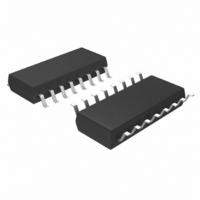
Physical Dimensions inches (millimeters) unless otherwise noted 16-Lead Small Outline Integrated Circuit (SOIC), JEDEC MS-012, 0.150 Narrow Package Number M16A 5 www.fairchildsemi.com ...

Page 6

Physical Dimensions inches (millimeters) unless otherwise noted (Continued) 16-Lead Small Outline Package (SOP), EIAJ TYPE II, 5.3mm Wide www.fairchildsemi.com Package Number M16D 6 ...

Page 7

Physical Dimensions inches (millimeters) unless otherwise noted (Continued) 16-Lead Plastic Dual-In-Line Package (PDIP), JEDEC MS-001, 0.300 Wide Fairchild does not assume any responsibility for use of any circuitry described, no circuit patent licenses are implied and Fairchild reserves the right ...

Related keywords