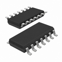
74HCT03D,653 NXP Semiconductors, 74HCT03D,653 Datasheet - Page 2

74HCT03D,653
Manufacturer Part Number
74HCT03D,653
Description
IC QUAD 2-IN NAND GATE 14SOIC
Manufacturer
NXP Semiconductors
Series
74HCTr
Datasheet
1.74HCT03D653.pdf
(8 pages)
Specifications of 74HCT03D,653
Number Of Circuits
4
Package / Case
14-SOIC (3.9mm Width), 14-SOL
Logic Type
NAND Gate
Number Of Inputs
2
Current - Output High, Low
4mA, 4mA
Voltage - Supply
4.5 V ~ 5.5 V
Operating Temperature
-40°C ~ 125°C
Mounting Type
Surface Mount
Product
NAND
Logic Family
HCT
High Level Output Current
- 4 mA
Low Level Output Current
4 mA
Propagation Delay Time
10 ns
Supply Voltage (max)
5.5 V
Supply Voltage (min)
4.5 V
Maximum Operating Temperature
+ 125 C
Mounting Style
SMD/SMT
Minimum Operating Temperature
- 40 C
Lead Free Status / RoHS Status
Lead free / RoHS Compliant
Lead Free Status / RoHS Status
Lead free / RoHS Compliant, Lead free / RoHS Compliant
Other names
568-4575-2
74HCT03D-T
74HCT03D-T
933748640653
74HCT03D-T
74HCT03D-T
933748640653
Philips Semiconductors
FEATURES
GENERAL DESCRIPTION
The 74HC/HCT03 are high-speed Si-gate CMOS devices
and are pin compatible with low power Schottky TTL
(LSTTL). They are specified in compliance with JEDEC
standard no. 7A.
QUICK REFERENCE DATA
GND = 0 V; T
Notes
1. C
2. For HC the condition is V
3. The given value of C
ORDERING INFORMATION
See
December 1990
t
C
C
PZL
SYMBOL
Level shift capability
Output capability: standard (open drain)
I
Quad 2-input NAND gate
I
PD
CC
f
f
V
C
V
R
For HCT the condition is V
C
/ t
i
o
“74HC/HCT/HCU/HCMOS Logic Package Information”
O
CC
PD
= input frequency in MHz
L
L
L
category: SSI
= output frequency in MHz
(C
(V
PLZ
= output load capacitance in pF
= pull-up resistor in M
= 0 pF and R
= output voltage in V
= supply voltage in V
O
is used to determine the dynamic power dissipation (P
L
P
2
D
/R
V
= C
L
amb
CC
) = sum of outputs
propagation delay
input capacitance
power dissipation capacitance per gate
PD
2
= 25 C; t
f
o
L
V
) = sum of outputs
=
CC
2
PD
r
PARAMETER
f
is obtained with:
i
= t
I
+
= GND to V
I
f
= GND to V
= 6 ns
(C
L
V
CC
CC
CC
2
f
o
1.5 V
) +
(V
O
C
notes 1, 2 and 3
2
L
/R
2
.
= 15 pF; R
L
)
The 74HC/HCT03 provide the 2-input NAND function.
The 74HC/HCT03 have open-drain N-transistor outputs,
which are not clamped by a diode connected to V
the OFF-state, i.e. when one input is LOW, the output
may be pulled to any voltage between GND and V
This allows the device to be used as a LOW-to-HIGH or
HIGH-to-LOW level shifter. For digital operation and
OR-tied output applications, these devices must have a
pull-up resistor to establish a logic HIGH level.
D
in W):
duty factor LOW, where:
CONDITIONS
L
= 1 k ; V
CC
= 5 V 8
3.5
4.0
HC
TYPICAL
Product specification
74HC/HCT03
HCT
3.5
4.0
10
ns
pF
pF
UNIT
CC
Omax
. In
.


