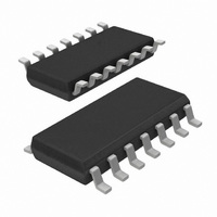
74LVC04AD,112 NXP Semiconductors, 74LVC04AD,112 Datasheet - Page 2

74LVC04AD,112
Manufacturer Part Number
74LVC04AD,112
Description
IC INVERTER HEX 5V TTL 14SOIC
Manufacturer
NXP Semiconductors
Series
74LVCr
Datasheet
1.74LVC04AD118.pdf
(15 pages)
Specifications of 74LVC04AD,112
Number Of Circuits
6
Logic Type
Inverter
Package / Case
14-SOIC (3.9mm Width), 14-SOL
Number Of Inputs
1
Current - Output High, Low
12mA, 12mA
Voltage - Supply
2.7 V ~ 3.6 V
Operating Temperature
-40°C ~ 125°C
Mounting Type
Surface Mount
Logic Family
74LVC
High Level Output Current
- 24 mA
Low Level Output Current
24 mA
Propagation Delay Time
14 ns
Supply Voltage (max)
3.6 V
Supply Voltage (min)
1.2 V
Maximum Operating Temperature
+ 125 C
Minimum Operating Temperature
- 40 C
Mounting Style
SMD/SMT
Operating Supply Voltage
1.2 V to 3.6 V
Lead Free Status / RoHS Status
Lead free / RoHS Compliant
Lead Free Status / RoHS Status
Lead free / RoHS Compliant, Lead free / RoHS Compliant
Other names
568-1573-5
74LVC04AD
935242400112
74LVC04AD
935242400112
NXP Semiconductors
4. Functional diagram
5. Pinning information
74LVC04A
Product data sheet
Fig 1.
Fig 4.
11
13
Logic symbol
Pin configuration SO14 and (T)SSOP14
1
3
5
9
1A
2A
3A
4A
5A
6A
GND
1A
1Y
2A
2Y
3A
3Y
5.1 Pinning
mna342
1
2
3
4
5
6
7
1Y
2Y
3Y
4Y
5Y
6Y
10
12
2
4
6
8
04
001aac915
14
13
12
11
10
9
8
All information provided in this document is subject to legal disclaimers.
V
6A
6Y
5A
5Y
4A
4Y
Fig 2.
CC
11
13
Rev. 7 — 1 February 2011
1
3
5
9
IEC logic symbol
1
1
1
1
1
1
mna343
Fig 5.
(1) The die substrate is attached to this pad using
2
4
6
8
10
12
conductive die attach material. It can not be used as a
supply pin or input.
Pin configuration DHVQFN14
index area
terminal 1
1Y
2A
2Y
3A
3Y
Fig 3.
Transparent top view
2
3
4
5
6
A
GND
04
Logic diagram for one gate
(1)
74LVC04A
13
12
11
10
9
001aac914
© NXP B.V. 2011. All rights reserved.
6A
6Y
5A
5Y
4A
Hex inverter
mna341
Y
2 of 15


