MC74HC03ADG ON Semiconductor, MC74HC03ADG Datasheet
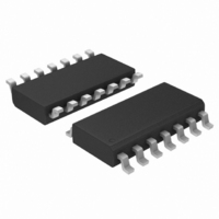
IC GATE NAND QUAD 2INP 14-SOIC

MC74HC03ADG

Manufacturer Part Number
MC74HC03ADG
Description
IC GATE NAND QUAD 2INP 14-SOIC
Manufacturer
ON Semiconductor
Series
74HCr
Datasheets

Specifications of MC74HC03ADG

Logic Type
NAND Gate with Open Drain
Number Of Inputs
2
Number Of Circuits
4
Current - Output High, Low
5.2mA, 5.2mA
Voltage - Supply
2 V ~ 6 V
Operating Temperature
-55°C ~ 125°C
Mounting Type
Surface Mount
Package / Case
14-SOIC (3.9mm Width), 14-SOL
Output Current
5.2mA
No. Of Inputs
2
Supply Voltage Range
2V To 6V
Logic Case Style
SOIC
No. Of Pins
14
Operating Temperature Range
-55°C To +125°C
Filter Terminals
SMD
Rohs Compliant
Yes
Family Type
HC
Lead Free Status / RoHS Status
Lead free / RoHS Compliant
Other names
MC74HC03ADG
MC74HC03ADGOS
MC74HC03A
Quad 2-Input NAND Gate
with Open-Drain Outputs
High−Performance Silicon−Gate CMOS
inputs are compatible with Standard CMOS outputs; with pullup
resistors, they are compatible with LSTTL outputs.
MOS N−Channel transistor. This NAND gate can, therefore, with a
suitable pullup resistor, be used in wired−AND applications. Having
the output characteristic curves given in this data sheet, this device can
be used as an LED driver or in any other application that only requires
a sinking current.
Features
© Semiconductor Components Industries, LLC, 2011
May, 2011 − Rev. 11
The MC74HC03A is identical in pinout to the LS03. The device
The HC03A NAND gate has, as its outputs, a high−performance
Resistor
Output Drive Capability: 10 LSTTL Loads With Suitable Pullup
Outputs Directly Interface to CMOS, NMOS and TTL
High Noise Immunity Characteristic of CMOS Devices
Operating Voltage Range: 2.0 to 6.0 V
Low Input Current: 1 mA
In Compliance With the JEDEC Standard No. 7 A Requirements
Chip Complexity: 28 FETs or 7 Equivalent Gates
These Devices are Pb−Free, Halogen Free and are RoHS Compliant
A
B
PIN 14 = V
PIN 7 = GND
* Denotes open-drain outputs
1,4,9,12
2,5,10,13
Pinout: 14−Lead Packages (Top View)
V
14
A1
CC
1
CC
B4
13
B1
2
LOGIC DIAGRAM
A4
12
Y1
3
Y4
A2
11
4
PROTECTION
OUTPUT
DIODE
B3
B2
10
5
A3
Y2
9
6
V
CC
GND
Y3
3,6,8,11
8
7
Y*
1
14
14
See detailed ordering and shipping information in the package
dimensions section on page 2 of this data sheet.
14
14
1
(Note: Microdot may be in either location)
1
1
Z = High Impedance
1
ORDERING INFORMATION
A
L, WL
Y, YY
W, WW
G or G
A
H
H
L
L
http://onsemi.com
FUNCTION TABLE
Inputs
CASE 948G
CASE 751A
SOEIAJ−14
TSSOP−14
DT SUFFIX
CASE 646
CASE 965
N SUFFIX
D SUFFIX
F SUFFIX
PDIP−14
SOIC−14
= Assembly Location
= Wafer Lot
= Year
= Work Week
= Pb−Free Package
B
H
H
L
L
Publication Order Number:
14
1
14
1
Output
DIAGRAMS
MC74HC03AN
14
AWLYYWWG
MARKING
14
1
MC74HC03A/D
Y
Z
Z
Z
L
1
AWLYWW
HC03AG
74HC03A
ALYWG
ALYWG
03A
HC
G

Related parts for MC74HC03ADG

MC74HC03ADG Summary of contents

Page 1

MC74HC03A Quad 2-Input NAND Gate with Open-Drain Outputs High−Performance Silicon−Gate CMOS The MC74HC03A is identical in pinout to the LS03. The device inputs are compatible with Standard CMOS outputs; with pullup resistors, they are compatible with LSTTL outputs. The HC03A ...

Page 2

... Internal Gate Power Dissipation Speed Power Product *Equivalent to a two−input NAND gate ORDERING INFORMATION Device MC74HC03ANG MC74HC03ADG MC74HC03ADR2G MC74HC03ADTR2G MC74HC03AFELG †For information on tape and reel specifications, including part orientation and tape sizes, please refer to our Tape and Reel Packaging Specifications Brochure, BRD8011/D. ...

Page 3

DC CHARACTERISTICS (Voltages Referenced to GND) Symbol Parameter V Minimum High−Level Input Voltage IH V Maximum Low−Level Input Voltage IL V Maximum Low−Level Output OL Voltage I Maximum Input Leakage Current in I Maximum Quiescent Supply CC Current (per Package) ...

Page 4

INPUT A 50% 10 PZL PLZ 90% OUTPUT Y 50% 10% t THL Figure 1. Switching Waveforms *The expected minimum curves are not guarantees, but are design ...

Page 5

−T− SEATING PLANE 0.13 (0.005) PACKAGE DIMENSIONS PDIP−14 N SUFFIX CASE 646−06 ISSUE http://onsemi.com 5 NOTES: 1. DIMENSIONING AND TOLERANCING ...

Page 6

G −T− SEATING 14 PL PLANE 0.25 (0.010 PACKAGE DIMENSIONS SOIC−14 D SUFFIX CASE 751A−03 ISSUE 0.25 (0.010 ...

Page 7

K 14X REF 0.10 (0.004) 0.15 (0.006 L PIN 1 IDENT. 1 0.15 (0.006 −V− C 0.10 (0.004) −T− G SEATING D PLANE 14X 0.36 PACKAGE DIMENSIONS TSSOP−14 DT SUFFIX ...

Page 8

... Opportunity/Affirmative Action Employer. This literature is subject to all applicable copyright laws and is not for resale in any manner. PUBLICATION ORDERING INFORMATION LITERATURE FULFILLMENT: Literature Distribution Center for ON Semiconductor P.O. Box 5163, Denver, Colorado 80217 USA Phone: 303−675−2175 or 800−344−3860 Toll Free USA/Canada Fax: 303− ...

Related keywords