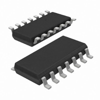
74LVC00AD,118 NXP Semiconductors, 74LVC00AD,118 Datasheet - Page 8

74LVC00AD,118
Manufacturer Part Number
74LVC00AD,118
Description
IC QUAD 2-IN NAND GATE 14-SOIC
Manufacturer
NXP Semiconductors
Series
74LVCr
Datasheet
1.74LVC00ADB118.pdf
(15 pages)
Specifications of 74LVC00AD,118
Number Of Circuits
4
Package / Case
14-SOIC (3.9mm Width), 14-SOL
Logic Type
NAND Gate
Number Of Inputs
2
Current - Output High, Low
24mA, 24mA
Voltage - Supply
2.7 V ~ 3.6 V
Operating Temperature
-40°C ~ 125°C
Mounting Type
Surface Mount
Product
NAND
Logic Family
74LVC
High Level Output Current
- 24 mA
Low Level Output Current
24 mA
Propagation Delay Time
6.5 ns
Supply Voltage (max)
3.6 V
Supply Voltage (min)
1.2 V
Maximum Operating Temperature
+ 125 C
Mounting Style
SMD/SMT
Minimum Operating Temperature
- 40 C
Package
14SO
Logic Function
NAND
Minimum Operating Supply Voltage
1.2 V
Maximum Operating Supply Voltage
3.6 V
Maximum Propagation Delay Time @ Maximum Cl
2.1(Typ)@3.3V ns
Logical Function
NAND
Number Of Elements
4
Operating Supply Voltage (typ)
1.8/2.5/3.3V
Operating Temp Range
-40C to 125C
Package Type
SO
Number Of Outputs
1
Technology
CMOS
Mounting
Surface Mount
Pin Count
14
Operating Temperature Classification
Automotive
Quiescent Current
40uA
Operating Supply Voltage (max)
3.6V
Operating Supply Voltage (min)
1.2V
Lead Free Status / RoHS Status
Lead free / RoHS Compliant
Lead Free Status / RoHS Status
Lead free / RoHS Compliant, Lead free / RoHS Compliant
Other names
568-2270-2
74LVC00AD-T
935249960118
74LVC00AD-T
935249960118
Philips Semiconductors
AC CHARACTERISTICS
GND = 0 V; t
Notes
1. Typical value is measured at V
2. Skew between any two outputs of the same package switching in the same direction. This parameter is guaranteed
AC WAVEFORMS
2003 Sep 04
T
t
t
T
t
t
SYMBOL
PHL
sk(0)
PHL
sk(0)
amb
amb
Quad 2-input NAND gate
V
V
V
by design.
M
M
OL
/t
/t
PLH
PLH
= 1.5 V at V
= 0.5V
= 40 to +85 C
= 40 to +125 C
and V
CC
OH
r
propagation delay
nA, nB to nY
skew
propagation delay
nA, nB to nY
skew
at V
are typical output voltage drop that occur with the output load.
= t
CC
CC
f
PARAMETER
< 2.7 V.
2.7 V;
2.5 ns.
handbook, halfpage
Fig.6 The input nA, nB to output nY propagation delays.
nA, nB input
CC
nY output
= 3.3 V.
see Figs 6 and 7 V
note 2
see Figs 6 and 7 V
note 2
WAVEFORMS
GND
V OH
V OL
V I
TEST CONDITIONS
V M
V
V
V
V
V
V
8
V M
CC
CC
CC
CC
CC
CC
CC
CC
t PHL
t THL
= 1.2
= 2.7
= 3.0 to 3.6
= 3.0 to 3.6
= 1.2
= 2.7
= 3.0 to 3.6
= 3.0 to 3.6
V
CC
(V)
1.0
1.0
1.0
1.0
MIN.
MNA218
t PLH
t TLH
12
2.4
2.1
TYP.
(1)
Product specification
5.1
4.3
1.0
6.5
5.5
1.5
MAX.
74LVC00A
ns
ns
ns
ns
ns
ns
ns
ns
UNIT


